Hold up – why are businesses and DIY creators suddenly obsessed with printing vivid galaxy patterns on cotton tees and metal phone cases? The answer lies in a game-changing technique revolutionizing modern customization.
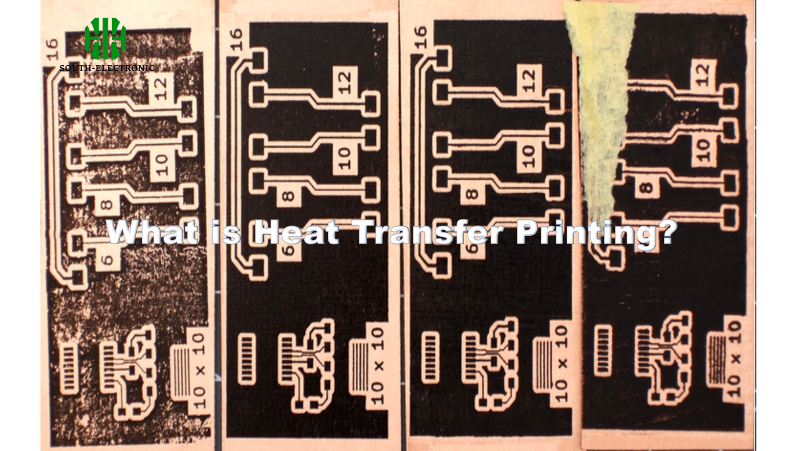
Heat transfer printing[^1] uses heat-activated adhesives to permanently bond digital designs onto fabrics, plastics, metals using transfer paper/film, offering low-cost, detailed customization for small batches[^2] without screen-printing setups.
When exploring printing methods, unexpected factors like material compatibility[^3] and environmental impact determine success. Let’s break down four critical aspects every creator should know before choosing this technique.
How Does Heat Transfer Printing Actually Work?
Ever wonder how that photorealistic unicorn image sticks perfectly to your kid’s backpack? The magic happens through calculated heat application.
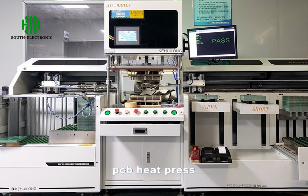
Printers first mirror-print designs on transfer paper using specialty inks. A heat press then applies precise temperature (300-400°F) and pressure (40-80 PSI) for 15-60 seconds to melt adhesive layers, bonding pigments to the target material permanently.
)
Three-Step Process Breakdown
While simple in concept, technical nuances make or break results:
| Step | Key Actions | Common Mistakes |
|---|---|---|
| Design Preparation | Mirror image creation, ICC color profiling | Forgetting to flip designs causing backward prints |
| Heat Application | Material-specific temperature calibration | Overheating polyester (causes yellowing) |
| Peeling Technique | Cold peel (vinyl) vs hot peel (sublimation) | Premature peeling causing incomplete transfers |
Material thickness dictates dwell time – a 2mm neoprene coaster needs 25% longer pressing than cotton aprons. Always test scraps first!
Heat Transfer vs Screen Printing: Which Is Better for Your Project?
Time-sensitive startup orders? Artistic experimentation? Let’s compare these titans through three real-world lenses.
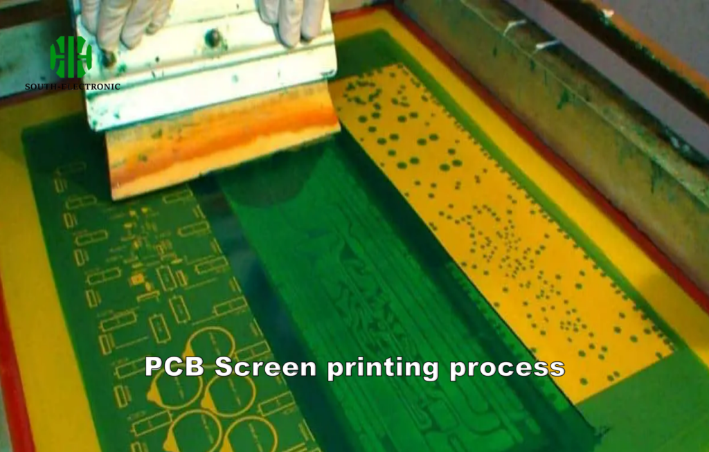
Choose heat transfer for prototypes/small batches (under 50 units) needing multicolor details. Opt for screen printing[^4] for large volumes of simple designs, prioritizing durability over intricate gradients.
)
Decision Matrix by Project Type
| Criteria | Heat Transfer Wins When… | Screen Printing Excels For… |
|---|---|---|
| Order Quantity | 1-100 pieces | 500+ units |
| Design Complexity | Photorealistic images | Bold 2-color logos |
| Turnaround Time | 24-hour rush jobs | 2-week production schedules |
| Fabric Type | Performance polyester | Heavyweight cotton canvas |
Remember: Heat transfers fade after 30-50 washes, while screen prints last longer. For gym apparel changed weekly, durability matters less than initial cost savings.
What Materials Work Best with Heat Transfer Printing?
Not all surfaces play nice with heat-activated adhesives. Performance fabrics and smooth synthetics rule here.
Cotton-polyester blends (50/50), ceramic tiles, anodized aluminum, and PVC-free plastics accept transfers best. Avoid natural rubber, silicone, and textured surfaces like burlap that prevent adhesive bonding.
)
Surface Prep Checklist
- Porosity Test – Spray water droplets. Immediate absorption = good for sublimation paper
- Heat Tolerance – Can handle 350°F for 45 seconds without warping?
-
Coating – Pre-treated vs untreated surfaces (requires different transfer films)
Pro Tip: Dark fabrics need opaque transfer papers (higher GSM) to prevent underlying color bleed-through. White/light materials use standard sheets.
Is Heat Transfer Printing Eco-Friendly?
With 92 million tons of annual textile waste, sustainability claims require scrutiny.
While water-based inks and recycled PET transfer films exist, most heat transfers involve plastic-coated papers ending in landfills. Eco-conscious creators[^5] should use compostable sheets[^6] and energy-efficient heat presses.
)
Environmental Impact Breakdown
| Aspect | Concern | Green Solutions |
|---|---|---|
| Energy Use | 1500W heat presses | Solar-powered presses |
| Waste Generation | Plastic transfer backing | Plant-starch based films |
| Chemical Runoff | PVC-containing transfers | OEKO-TEX certified adhesives |
| Longevity | Shorter lifespan = more waste | Double-sided sealing machines |
For true sustainability, pair eco-transfers with organic substrates like GOTS-certified cotton[^7]. Every element matters.
Conclusion
Heat transfer printing democratizes custom manufacturing – turning kitchen tables into microfactories. Match materials wisely, prioritize small batches, and while not perfectly green, smarter choices reduce ecological footprint. Your imagination’s now the main limit.
[^1]: Explore this link to understand the fundamentals of heat transfer printing and its applications in customization.
[^2]: Discover strategies for effective small batch customization that can enhance your business offerings.
[^3]: Learn about the significance of material compatibility in printing to ensure successful results and avoid common pitfalls.
[^4]: Learn why screen printing is preferred for large orders and how it ensures durability and quality in designs.
[^5]: Explore how eco-conscious creators are making sustainable choices in heat transfer printing to reduce environmental impact.
[^6]: Learn about the advantages of compostable sheets and how they contribute to a more sustainable printing process.
[^7]: Discover the significance of GOTS-certified cotton in promoting eco-friendly practices in the textile industry.

