+86 4008783488

20240617-151702

Via-In-Pad in PCB Design: A Comprehensive Guide

Via-in-pad technology enhances PCB design by improving signal integrity, thermal management, and space efficiency, crucial for modern electronics. Despite higher costs and manufacturing challenges, its advantages make it pivotal for advanced devices. As processes improve, its adoption is expected to rise, revolutionizing electronic design further.
Get in touch

Where Are We?

Factory Address

Industrial Park, No. 438, Shajing Donghuan Road, Bao'an District, Shenzhen, Guangdong, China

Head Office Address

Floor 4, Zhihui Creative Building, No.2005 Xihuan Road, Shajing, Baoan District, Shenzhen, China

HK Office Address

ROOM A1-13,FLOOR 3,YEE LIM INDUSTRIAL CENTRE 2-28 KWAI LOK STREET, KWAI CHUNG HK,CHINA

Let's Talk

Phone : +86 400 878 3488

Send Us A Message

The more detailed you fill out, the faster we can move to the next step.

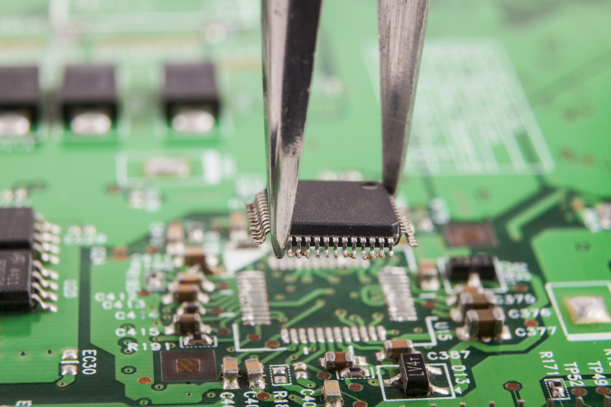
Microchip Removal