Your Premier PCB Assembly Partner
South-Electronic
At South-Electronic, we understand the critical importance of precision and reliability in PCB assembly, which is why we offer advanced solutions tailored to meet the specific needs of your projects.
Work with us to get your electronics manufacturing
Surface Mount Technology (SMT)
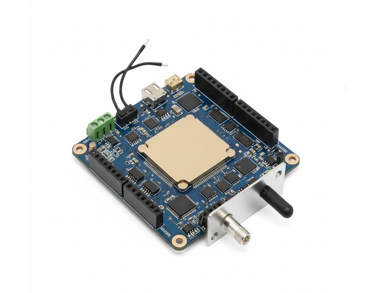
These circuit boards are central to managing the engine's operations such as fuel injection, ignition timing, and emissions control. They must be highly reliable and able to withstand harsh environmental conditions.
Through-Hole Technology (THT)
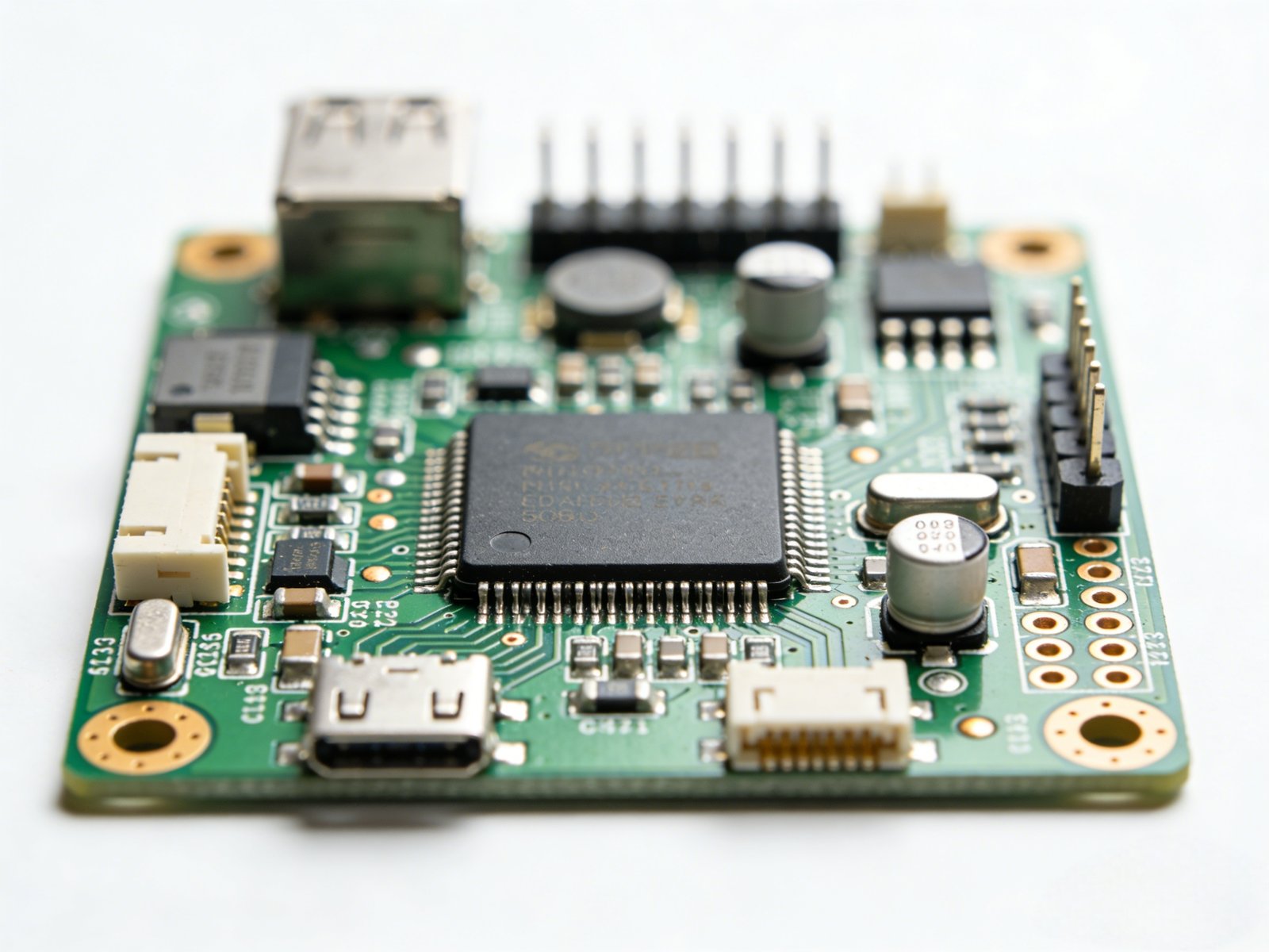
Responsible for various body-related functions such as lighting, power windows, central locking, and other convenience features. BCMs often require multiple interfaces for sensors and actuators throughout the vehicle.
Mixed Technology Assembly
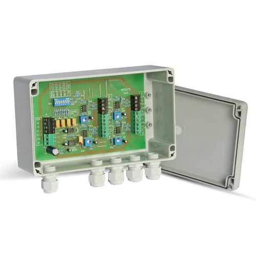
These handle audio and video entertainment, navigation, and connectivity functions like Bluetooth and Wi-Fi. They often support sophisticated user interfaces and high-speed data processing
Prototype Assembly:
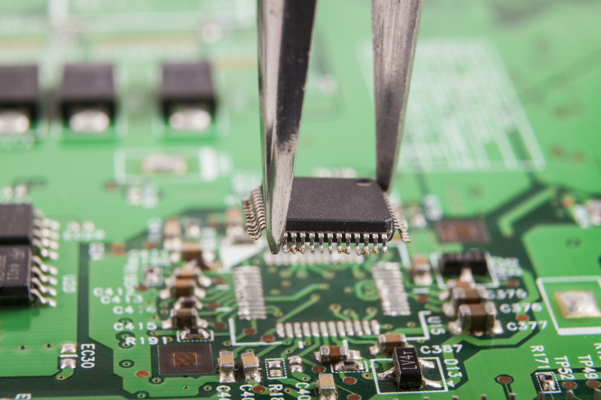
This category includes circuit boards for airbag systems, antitheft systems, and other safety-related features that require quick response times and fail-safe operation.
Why Choose South-Electronic?
Choose South-Electronic for our expertise in delivering custom, high-quality PCB assemblies for a wide range of applications. Our team has extensive experience, ensuring superior quality at competitive prices and exceptional service from start to finish.
- Flexibility in Ordering
Your projects deserve flexibility.
No matter the size of your order, you can order as little as one piece. We make sure that your specific assembly needs are met without compromise. - Experienced Team
Your success is backed by expertise.
Benefit from over a decade of industry experience from our dedicated team, committed to delivering excellence in every project. - Comprehensive Service
Your satisfaction is our priority.
Our extensive range of equipment and meticulous assembly processes guarantee that every order meets your exact requirements. - Fast Delivery
Your deadlines are important to us. .
Our efficient production and operations ensure quick turnaround times, allowing you to meet tight schedules without sacrificing quality. - Rapid Response and Delivery
Your deadlines are important, and we meet them.
With our efficient production processes and optimized logistics, we ensure timely delivery of your orders. - Guaranteed Satisfaction
Your peace of mind is guaranteed..
As an ISO9001 certified factory, we are committed to delivering top-quality products and maintaining clear communication.
Related Project We had Done
Customer Reviews
engineer
thank you, guys, the boards are really good, i am really happy to receive my boards, the components are perfect!
Operation Manager
South-Electronic is my first PCBA supplier in China. The service and quality are excellent, and the after-sales support is also very impressive. Good Job!
Common Questions
Most Popular Questions
PCB Assembly refers to the process of mounting electronic components onto a printed circuit board. This process can involve various techniques such as Surface Mount Technology (SMT) and Through-Hole Technology (THT).
The primary steps include component procurement, PCB fabrication, component placement, soldering, inspection, and functional testing. Each step requires precise technology and strict quality control to ensure high standards.
South-Electronic offers customized, high-quality PCB assembly services backed by over a decade of industry experience, ISO9001-certified production facilities, and efficient production operations to ensure product quality and prompt delivery.
Yes, South-Electronic supports orders starting from a minimum order quantity (MOQ) of just one piece, accommodating everything from prototypes to large-scale production.
3 Days at the fastest. Delivery times vary depending on the scale and specifics of the order. We strive to optimize our production processes to complete orders within the shortest possible timeframes.
You can initiate a project by contacting us through our website or by directly emailing info@southelectronicpcb.com. Our customer service team will discuss your project requirements and the next steps with you.
Yes, we provide comprehensive services from design to production, including PCB design optimization and recommendations to ensure manufacturability and functionality.
Common issues include incorrect component placement and soldering problems. South-Electronic prevents and resolves these issues through the use of advanced equipment, rigorous production controls, and comprehensive quality testing and auditing.
South-Electronic provides comprehensive support during the design and manufacturing process, including consultation on design optimization, material selection, and prototype testing to ensure your product meets all expectations and industry standards.
Send us a message
The more detailed you fill out, the faster we can move to the next step.
The Complete Guide For PCB Assembly
Contents
Chapter 1
Introduction to PCB Assembly
Overview of PCB Assembly
Printed Circuit Board (PCB) Assembly is a critical process in the manufacturing of electronic devices, involving the placement and soldering of various electronic components onto a PCB. This process is fundamental to the production of virtually all electronic hardware, as it enables the integration of the necessary components that allow devices to perform their intended functions. The assembly process can utilize various technologies, most notably Surface Mount Technology (SMT) and Through-Hole Technology (THT). Each technique offers different advantages and is chosen based on the requirements of the electronic device being produced.
In PCB Assembly, components such as resistors, capacitors, and integrated circuits are precisely placed on the board according to the circuit design. The process involves several steps, starting from applying solder paste to the board, placing components, soldering, inspection, and testing to ensure functionality. Modern PCB Assembly is highly automated with the use of sophisticated equipment like pick-and-place machines, reflow ovens, and automated inspection machines that enhance accuracy and efficiency.
Importance in Electronics Manufacturing
PCB Assembly is indispensable in electronics manufacturing due to its impact on the functionality, reliability, and performance of electronic products. A well-assembled PCB ensures that the electronic device operates as intended under various conditions. The quality of PCB Assembly directly affects the overall quality of the electronic product, influencing factors such as lifespan, safety, and user satisfaction.
Moreover, PCB Assembly plays a significant role in the innovation of electronics. As devices become smaller, more powerful, and more integrated, the assembly process must adapt to handle the increasing complexity and miniaturization of components. Advanced PCB Assembly allows for the development of compact, high-performance devices such as smartphones, wearables, and medical devices, pushing the boundaries of what electronic devices can achieve.
Furthermore, PCB Assembly impacts cost-efficiency and scalability in manufacturing. Efficient assembly processes can reduce production costs and time-to-market, enabling companies to respond more swiftly to market demands and technological advancements. In the competitive electronics industry, mastering PCB Assembly techniques can provide manufacturers with a significant advantage, allowing them to produce high-quality products at competitive prices.
In summary, PCB Assembly is a cornerstone of electronics manufacturing, playing a crucial role in determining the quality, innovation, and economic efficiency of electronic products. Its significance extends beyond mere manufacturing, influencing the technological advancement and competitiveness of companies in the global electronics market.
Chapter 2
Key Components of PCB Assembly
Printed Circuit Boards (PCBs)
Printed Circuit Boards (PCBs) are the backbone of any electronic device. They provide the physical platform on which electronic components are mounted and are responsible for the routing of electrical signals between these components. PCBs are made from layers of insulating material with copper pathways etched onto them, which conduct electricity. The design and layout of these pathways are crucial as they directly affect the functionality and performance of the assembled board. PCBs can vary greatly in complexity, from simple single-layer boards used in basic devices to intricate multi-layer boards found in advanced computing and telecommunications equipment.
Electronic Components
Electronic components are the active and passive elements that are mounted on the PCB to perform specific functions within an electronic circuit. These include:
- Active components such as integrated circuits (ICs), microprocessors, and transistors, which drive the functionality of electronic devices by processing signals and performing computations.
- Passive components such as resistors, capacitors, and inductors, which support the circuit operations by controlling voltage and current flows.
The selection of these components is critical as it determines the capabilities and limits of the electronic device. Components are chosen based on factors like power requirements, signal frequency, and environmental conditions under which the device will operate.
Soldering Materials
Soldering materials are essential in PCB Assembly for making reliable electrical connections between the components and the board. The most common soldering material used is solder paste, a mix of flux and solder particles. The flux helps in cleaning the metal surfaces during the soldering process, which is vital for forming strong and conductive bonds. Solder paste is typically applied to the board using a stencil before the components are placed and then melted in a process called reflow soldering to establish connections.
Besides solder paste, other materials such as solder wire and solder balls are also used, particularly in through-hole technology and ball grid array (BGA) package assemblies, respectively. The choice of soldering material depends on the assembly technique and the specific requirements of the electronic device, including considerations for strength, conductivity, and resistance to environmental factors.
Each of these key components plays a vital role in PCB Assembly. The PCB provides the structure, the electronic components add functionality, and the soldering materials secure the components in place and ensure connectivity. The careful selection and handling of these components are fundamental to the successful assembly of reliable and effective electronic devices.
Chapter 3
Technologies in PCB Assembly
Surface Mount Technology (SMT)
Surface Mount Technology (SMT) is a widely used PCB assembly method where components are mounted directly onto the surface of the PCB without the need for large drilled holes. Components used in SMT, known as surface mount devices (SMDs), are smaller than their through-hole counterparts, allowing for a higher density of components on the board. This technology not only facilitates the miniaturization of devices but also enhances the electrical performance due to shorter electrical paths.
The SMT process typically involves the application of solder paste to the PCB using a stencil to outline the pads where components will be placed. A pick-and-place machine then precisely places the SMDs onto the solder-pasted pads. The board with placed components passes through a reflow oven where the solder paste melts and solidifies, creating permanent solder joints. SMT is favored for its speed and automation, which significantly reduce assembly time and cost, especially suitable for high-volume production.
Through-Hole Technology (THT)
Through-Hole Technology (THT) involves the insertion of component leads into pre-drilled holes on the PCB. Once the components are in place, soldering is performed either manually or using a wave soldering machine which bathes the exposed leads in molten solder. THT is noted for providing strong mechanical bonds, making it ideal for components that need to withstand physical stress or mechanical loads, such as connectors and large capacitors.
Although THT is generally less efficient in terms of space utilization and labor compared to SMT, it remains indispensable for certain applications requiring robust physical connections and enhanced reliability under stress. It is also preferred when prototyping or in applications where repairs and modifications need to be made frequently.
Mixed Technology Assembly
Mixed technology assembly involves the use of both SMT and THT techniques on the same PCB. This approach combines the advantages of both technologies: the high density and efficiency of SMT and the mechanical robustness of THT. Mixed assembly is often used in complex electronics such as computer motherboards, industrial equipment, and mixed-signal devices, where both high component density and strong mechanical bonds are necessary.
During mixed technology assembly, SMT components are usually placed and reflow-soldered first. Following this, THT components are inserted and soldered using selective soldering techniques that avoid damaging the already soldered SMT components. This process requires careful planning and design to ensure compatibility and functionality across both assembly methods.
The choice of assembly technology—SMT, THT, or mixed—depends on the specific requirements of the electronic device, including factors such as component density, physical size, mechanical strength, and production volume. Each technology has its own set of advantages and applications, making them essential to the diverse needs of modern electronics manufacturing.
Chapter 4
The PCB Assembly Process
Step-by-Step Guide
The PCB assembly process is a detailed and precise operation involving several critical steps, each contributing to the functionality and reliability of the final product. Here’s a comprehensive step-by-step guide to the process:
PCB Design and Output: Before any physical assembly begins, the PCB design is finalized using computer-aided design (CAD) software. This design is then converted into a format suitable for manufacturing, typically in Gerber file format, which serves as a blueprint for the production process.
Material Procurement: All necessary materials, including the PCB itself and electronic components needed for the assembly, are procured. This stage requires strict quality checks to ensure all parts meet the required specifications.
Solder Paste Application: For SMT assembly, solder paste is applied to areas of the PCB where components will be placed. This is typically done using a stencil that matches the PCB design, ensuring that solder paste is only applied where needed.
Pick and Place: Automated machines, known as pick-and-place machines, are used to place surface mount components on the PCB. These machines are highly accurate and can place hundreds or thousands of components per hour.
Reflow Soldering: Once components are placed, the PCB passes through a reflow oven. The temperature of the oven is carefully controlled to melt the solder paste, which solidifies to form a strong electrical and mechanical connection between the components and the board.
Through-Hole Component Insertion: For PCBs requiring THT components, these are inserted manually or by automated insertion machines into pre-drilled holes on the PCB.
Wave Soldering: For soldering through-hole components, the PCB is passed over a wave soldering machine where molten solder coats the bottom of the board and bonds the THT components in place.
Inspection and Quality Control: After soldering, the boards are inspected for solder quality, component placement, and other potential defects. Inspection techniques include manual checks, automatic optical inspection (AOI), and X-ray inspection for hidden joints.
Testing: Functional tests are conducted to ensure the PCB performs as intended. This may involve power-up tests, in-circuit tests (ICT), and functional testing using specific test equipment.
Final Assembly: Additional mechanical assembly, including casing, screws, and final wiring, is completed, followed by final testing and quality assurance checks.
Packaging and Shipping: Once assembly and testing are complete, the PCBs are packaged securely and prepared for shipping to the customer or the next stage of product assembly.
Equipment Used in Assembly
Several types of specialized equipment are utilized throughout the PCB assembly process, each serving a distinct function:
- Stencil Printer: Applies solder paste to the PCB using a stencil that matches the PCB design.
- Pick-and-Place Machine: Automatically places SMT components on the PCB.
- Reflow Oven: Heats the PCB to melt the solder paste and form solder joints.
- Wave Soldering Machine: Used for soldering through-hole components by passing the PCB over a wave of molten solder.
- Automatic Optical Inspection (AOI) Machine: Checks for soldering faults and component placement errors.
- X-Ray Inspection Equipment: Used to inspect solder joints and component placement that are not visible externally.
- In-Circuit Test (ICT) Equipment: Checks the electrical performance of the PCB to ensure all components function correctly.
- Functional Test Rigs: Custom setups that simulate the operating environment of the PCB to ensure it performs as expected.
The combination of these steps and equipment ensures that PCB assembly is carried out with high precision and quality, leading to reliable and high-performing electronic devices.
Chapter 5
Design Considerations for PCB Assembly
Design for Manufacturing (DFM)
Design for Manufacturing (DFM) in the context of PCB assembly involves adapting the PCB design to streamline the manufacturing process, reduce costs, and ensure the reliability of the assemblies. DFM aims to identify potential production issues early in the design phase to mitigate risks associated with component placement, soldering, and assembly processes. Key aspects of DFM for PCBs include:
- Component Placement: Designers should optimize the layout to facilitate easy placement of components, ensuring that there is adequate space for automated pick-and-place machines to operate. Components should be aligned to minimize the movements of assembly machines.
- Solderability: Ensuring that pads are designed to the correct size and spacing to prevent solder bridging or insufficient solder joints during the reflow process.
- Panelization: Designing the PCB to fit within a standard panel size can maximize the number of boards produced per panel, reducing material waste and cost.
- Testability: Including features like test points and probe-able vias in the PCB design allows for easier access during testing phases, such as In-Circuit Tests (ICT).
PCB Layout Tips
A well-thought-out PCB layout is crucial for the functionality and manufacturability of the final product. Some practical tips for PCB layout include:
- Consistent Component Orientation: Align similar components in the same direction as much as possible. This alignment reduces the time and complexity of the assembly process and minimizes errors.
- Use of Adequate Trace Widths: Ensuring trace widths are adequate to handle the current load can prevent overheating and reduce the risk of trace failure.
- Minimize Trace Lengths: Shorter traces reduce the risk of signal degradation, especially important in high-frequency or high-speed circuits.
- Avoid Sharp Turns: Smooth, rounded traces are preferable as sharp turns can lead to increased resistance and potential points of failure.
- Decoupling Capacitors: Place them close to the power pins of integrated circuits to help stabilize the power supply and reduce noise.
Thermal and Mechanical Considerations
Thermal and mechanical stresses can affect PCB performance and lifespan, so it’s important to consider these factors during the design stage:
- Thermal Management: Incorporate heat sinks, thermal vias, and appropriate spacing for heat dissipation, especially for high-power components. The layout should facilitate airflow around heat-generating components to prevent hotspots.
- Mechanical Strength: For PCBs that will encounter mechanical stress or need to support heavy components, consider using thicker boards or additional support structures like mounting holes or brackets.
- Material Selection: Choosing the right substrate material can affect both the thermal and mechanical properties of the PCB. For example, materials like FR4 are standard for rigid boards, but high-temperature applications might require more advanced materials such as polyimide.
By integrating these design considerations into the PCB design process, manufacturers can significantly enhance the manufacturability, functionality, and reliability of their products. These practices not only improve product quality but also contribute to smoother, more efficient production workflows.
Chapter 6
Prototyping in PCB Assembly
Importance of Prototyping
Prototyping is a crucial phase in the PCB assembly process, serving as a preliminary model to evaluate and refine the functionality of an electronic device before full-scale production begins. It allows designers and engineers to:
- Identify Design Flaws: Early detection of design issues, such as incorrect component placement or inadequate trace widths, can save significant time and resources by avoiding costly rework during mass production.
- Test Functionality: Prototypes provide a working version of the PCB that can be tested in real-world conditions to ensure it meets all operational requirements.
- Gather User Feedback: Early-stage prototypes can be used to gather feedback from stakeholders or potential customers, which can be invaluable in refining the product design.
- Compliance and Certification: Testing prototypes helps ensure that the final product will comply with industry standards and regulatory requirements, which is crucial for market acceptance.
Rapid Prototyping Techniques
Rapid prototyping techniques enable the quick physical realization of PCB designs, allowing for faster iterations and more immediate evaluation. Some common methods include:
- 3D Printing: While traditionally used for enclosures and product casings, advancements in 3D printing technology now allow for the printing of conductive materials, enabling the creation of PCB prototypes with integrated conductive traces.
- Laser Cutting and CNC Milling: These methods can be used to quickly produce PCB substrates and conductive layers, albeit generally for simpler circuit designs.
- Solder Paste Stenciling and Reflow: For more complex prototypes, applying solder paste with a stencil to a standard PCB, placing components manually or with a pick-and-place machine, and then reflowing solder is an effective method to assemble prototypes that closely mimic the final product.
Testing and Evaluation
Once a prototype is assembled, it undergoes rigorous testing and evaluation to ensure it performs as intended. Key aspects include:
- Electrical Testing: Includes power-on tests, functionality tests, and signal integrity measurements. Tools like oscilloscopes and multimeters are commonly used to diagnose issues and verify performance against design specifications.
- Environmental Testing: Subjects the prototype to various environmental conditions such as temperature extremes, humidity, and mechanical stress to ensure operational robustness.
- User Testing: Involves allowing end-users to interact with the prototype, providing insights into usability and identifying any potential issues not apparent to the designers.
- Iterative Refinement: Based on testing outcomes, the design may be modified and retested. This iterative process continues until the prototype meets all the specified requirements.
Prototyping is an indispensable step in PCB assembly, providing critical insights that refine product design and functionality. By employing rapid prototyping techniques and thorough testing protocols, manufacturers can significantly enhance the development speed and success rate of new electronic devices.
Chapter 7
Quality Control and Testing
Inspection Techniques
Inspection is a critical component of the quality control process in PCB assembly, ensuring that each board meets stringent quality standards before it moves on to the next phase or is delivered to the customer. Modern PCB inspection employs several techniques:
Visual Inspection: Often the first line of defense, visual inspections are conducted by skilled technicians or using automated optical inspection (AOI) systems that use high-resolution cameras to detect a wide range of surface defects such as misalignments, solder quality, and component placement errors.
Automated Optical Inspection (AOI): AOI is crucial for verifying solder paste application, component placement, and solder joint quality on PCBs. It can quickly identify issues such as bridging, insufficient solder, and component skew.
X-Ray Inspection: This technique is used for examining hidden features of the PCB, such as beneath BGA (Ball Grid Array) packages. X-ray inspection can identify issues like solder voids and BGA alignment, which are not visible to the naked eye or AOI.
In-Circuit Testing (ICT): ICT involves testing the populated board via test points to check for shorts, opens, resistance, capacitance, and other basic quantities to ensure the functionality of each component on the board.
Functional Testing
Functional testing involves verifying that the PCB performs according to its design specifications under typical or extreme operating conditions. This phase of testing might include:
Power-Up Tests: Ensuring the board powers up correctly without issues such as shorts, overcurrent, or functionality failures.
Signal Integrity Testing: Evaluating the signal quality across critical paths to ensure high-speed signals are not degraded by the layout or component issues.
Software and Firmware Loading: Testing the board with the intended software or firmware to make sure it interacts correctly with the hardware.
System-Level Testing: Incorporating the PCB into the complete system to see if it interacts as expected with other system components.
Reliability Tests
Reliability testing is designed to challenge the PCB and its components under various stress conditions to simulate the life cycle of the product. These tests are crucial for determining the durability and lifespan of the PCB assembly:
Temperature Cycling: Subjecting the PCB to extreme temperatures in rapid succession to identify potential failures caused by thermal expansion and contraction.
Vibration and Shock Tests: Testing how well the PCB can withstand physical stress, which is particularly important for devices intended for transportation or industrial applications.
Humidity Testing: Exposing the PCB to high levels of humidity to ensure that moisture does not lead to corrosion or other failures.
Highly Accelerated Life Testing (HALT): This is an intense testing process that uses extreme stress conditions to rapidly find the limits of a product.
Quality control and testing are essential aspects of the PCB assembly process, ensuring that every board is built to meet both the functional specifications and the long-term reliability expected by customers. By implementing thorough inspection, functional testing, and reliability testing protocols, manufacturers can maintain high-quality standards and minimize the risk of product failures in the field.
Chapter 8
Common Issues and Troubleshooting
Frequent Assembly Problems
PCB assembly can encounter a range of common issues that can affect the functionality and quality of the final product. Understanding these problems is crucial for effective troubleshooting and quality control:
- Solder Bridging: Occurs when solder connects two or more pins that should not be connected, potentially causing shorts.
- Insufficient or Excessive Solder: Leads to weak joints or shorts, respectively. Insufficient solder may not form a reliable electrical connection, while excessive solder can overflow and cause bridging.
- Misaligned or Incorrectly Placed Components: Components that are not placed correctly can lead to non-functional circuits or create short circuits.
- Tombstoning: A phenomenon where one end of a two-pin component lifts off the board during soldering, usually due to uneven heating or imbalanced solder paste application.
- Open Circuits: Can occur if a component fails to bond with the board during the soldering process, often due to dirty component leads or PCB pads.
- Pad Lifting: Happens when a pad detaches from the PCB during the soldering or de-soldering process, which can damage the board irreparably.
Troubleshooting Tips
When faced with assembly issues, the following troubleshooting tips can help identify and resolve problems efficiently:
- Visual Inspection: Use magnification and strong lighting to inspect suspected areas closely. Look for signs of poor soldering, misalignment, and damage to components or PCB traces.
- Reflow Profile Adjustment: Adjust the temperature profile of reflow soldering processes to ensure even heating and appropriate solder flow.
- Use of Non-Contact Inspection Tools: Tools like AOI and X-ray inspection provide deeper insights into issues like solder bridging or hidden layer defects without needing to physically interact with the delicate components.
- Resoldering: In cases of insufficient solder, applying additional solder can sometimes rectify weak joints. Conversely, excess solder can be removed using a solder wick or vacuum tool.
- Component Realignment and Replacement: Misaligned components should be repositioned correctly, and any faulty components should be replaced promptly to avoid further issues.
Preventive Measures
Implementing preventive measures can significantly reduce the incidence of common PCB assembly problems:
- Design for Manufacturability (DFM): Incorporate DFM principles from the outset to minimize potential assembly issues. This includes optimizing pad sizes, component placement, and trace routing.
- Quality Control at Every Stage: Implement quality checks at each stage of the assembly process—from incoming material inspection to post-assembly testing.
- Proper Training for Assembly Staff: Ensure that all personnel are trained on the latest assembly techniques and are aware of common pitfalls.
- Regular Equipment Maintenance: Keep all assembly machinery and tools well-maintained to ensure they operate at optimal efficiency and accuracy.
- Feedback Loop: Establish a feedback loop from the testing and quality control phases back to design and procurement to continually improve the process based on real-world data.
By understanding these common issues, applying effective troubleshooting techniques, and implementing robust preventive measures, manufacturers can significantly enhance the reliability and efficiency of the PCB assembly process.
Chapter 9
Advancements in PCB Assembly Technology
Automation in Assembly
The integration of automation into PCB assembly processes has dramatically increased efficiency, accuracy, and consistency while reducing labor costs and human error. Key developments in automation include:
- Automated Pick-and-Place Machines: These machines use vacuum nozzles to pick up and precisely place components on the PCB. Advanced models are equipped with vision systems to adjust component placement in real-time, ensuring high accuracy even at very high speeds.
- Automatic Solder Paste Printing: Automated systems apply solder paste with high precision using stencils that match the PCB layout, which significantly reduces the chances of solder faults like bridging or insufficient solder.
- Reflow Ovens with Automated Profiling: Modern reflow ovens automatically adjust temperature profiles based on the board and solder type, improving the quality of solder joints and reducing defects.
- Automated Inspection Systems: Tools such as AOI (Automated Optical Inspection) and AXI (Automated X-ray Inspection) are now essential for checking assembly quality without slowing down production, providing real-time feedback that can be used to fine-tune the assembly process.
Emerging Technologies and Materials
As PCBs become more complex and performance demands increase, emerging technologies and materials are being adopted to meet these challenges:
- Flexible and Rigid-Flex PCBs: These boards combine rigid and flexible substrates, allowing for more versatile designs that can fit into unconventional spaces and improve durability by reducing the number of connectors and interconnections.
- Advanced Substrate Materials: Materials like high-frequency laminates, ceramic-based substrates, and thermally enhanced materials are being used to improve signal integrity, reduce electromagnetic interference (EMI), and manage heat more effectively in high-performance electronics.
- 3D Printing for PCBs: Additive manufacturing is being explored for its potential to print entire PCBs or to add conductive traces directly onto non-traditional substrates, opening up new possibilities in custom and on-demand electronics manufacturing.
Future Trends in PCB Assembly
Looking ahead, several trends are likely to shape the future of PCB assembly:
- Integration of AI and Machine Learning: AI is expected to play a significant role in further optimizing PCB assembly processes. Machine learning algorithms can predict and detect potential failures before they occur by analyzing data collected from sensors and inspection systems.
- Environmentally Friendly Processes: As sustainability becomes more critical, the industry is moving towards lead-free solders, recycling-friendly components, and methods that reduce waste and energy consumption.
- Smarter, More Connected Factories: The concept of Industry 4.0, with fully connected and automated factories that communicate internally and with other parts of the supply chain, is becoming a reality. This connectivity will allow for more responsive and adaptable manufacturing environments.
- Augmented Reality (AR) in Assembly: AR tools can assist in manual assembly processes by overlaying information like component placement diagrams and detailed instructions directly into the worker’s field of view, reducing errors and improving training.
Advancements in PCB assembly technology not only drive innovation in electronic device manufacturing but also ensure that the industry can meet the increasing demands for faster, smaller, and more reliable electronics.
Chapter 10
Choosing the Right PCB Assembly Partner
Criteria for Selecting a PCB Assembler
Selecting the right PCB assembly partner is crucial for ensuring the success of your electronics projects. Here are key criteria to consider when evaluating potential partners:
- Capabilities and Services: Ensure the assembler can meet your specific requirements, whether you need low-volume prototyping or high-volume production. Check if they offer the technologies you require, such as SMT, THT, or mixed assembly services.
- Quality Assurance and Standards Compliance: Look for an assembler with robust quality management systems in place. Certifications such as ISO 9001, ISO 13485 for medical devices, or automotive-specific certifications like IATF 16949 indicate a commitment to maintaining high standards.
- Lead Times and Flexibility: Evaluate the assembler’s ability to meet your timelines. Flexibility in handling last-minute changes and their ability to scale up or down quickly is also crucial.
- Supply Chain and Component Sourcing: A good assembly partner will have established relationships with component suppliers and the ability to manage supply chain issues, which is particularly important in times of component shortages.
Cost Considerations
Cost is always a significant factor in selecting a PCB assembly partner, but it should be balanced with quality and service:
- Quotation Transparency: Ensure the quotes provided are detailed and transparent, breaking down costs such as material, labor, tooling, and any additional charges.
- Volume Discounts: Discuss volume discounts for large orders. A good partner should offer scaled pricing that benefits both parties in high-volume runs.
- Long-term Cost Savings: Consider the long-term cost benefits associated with high-quality production. A slightly higher upfront cost might result in fewer reworks and lower failure rates, which saves money over the product’s lifecycle.
Evaluating Expertise and Certifications
The expertise and certifications of a PCB assembly partner are indicative of their ability to deliver high-quality services:
Technical Expertise: Assess the technical proficiency of the team. Look at the tenure and background of the engineering and production staff. A knowledgeable team can provide invaluable input during the design phase to improve manufacturability and reduce costs.
Certifications: Certifications can provide a benchmark for the assembler’s commitment to quality and compliance with industry standards. Common certifications include:
- ISO 9001: General quality management system standard that shows a commitment to consistent quality and continuous improvement.
- ISO 13485: Essential for assemblies used in medical devices, indicating compliance with stringent quality standards.
- AS9100: Pertinent for aerospace applications, reflecting standards that satisfy Department of Defense, NASA, and FAA quality requirements.
- RoHS, REACH Compliance: Indicates adherence to environmental regulations, which is crucial for selling electronic products in certain markets.
Case Studies and References: Ask for case studies or references from projects similar to yours. Feedback from current or past clients can provide real insights into the assembler’s capabilities and reliability.
Choosing the right PCB assembly partner is a strategic decision that impacts not only the cost and quality of your product but also its success in the market. It’s essential to consider a mix of technical capabilities, cost efficiency, and proven track record to ensure that your electronic projects are delivered to the highest standards.
Get in touch
Where Are We?
Industrial Park, No. 438 Donghuan Road, No. 438, Shajing Donghuan Road, Bao'an District, Shenzhen, Guangdong, China
Floor 4, Zhihui Creative Building, No.2005 Xihuan Road, Shajing, Baoan District, Shenzhen, China
ROOM A1-13,FLOOR 3,YEE LIM INDUSTRIAL CENTRE 2-28 KWAI LOK STREET, KWAI CHUNG HK
service@southelectronicpcb.com
Phone : +86 400 878 3488
Send us a message
The more detailed you fill out, the faster we can move to the next step.