
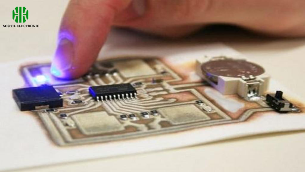
3D printed circuit boards (PCBs) are electronic circuits produced using additive manufacturing techniques, which involve the 3D print of electronic components. This innovative approach offers significant advantages, including cost reduction and design flexibility, making it increasingly popular across various industries.
What are 3D Printed Circuit Boards?
3D printed circuit boards (PCBs) are electronic circuits produced using additive manufacturing techniques. Unlike traditional PCBs, which are typically made by etching copper on a substrate, 3D printed PCBs are created by layering conductive materials, such as metals or conductive filaments, to form the desired circuit pattern. This innovative approach allows for greater design flexibility and customization.
These printed circuit boards can be used in a variety of applications, including consumer electronics, electrical appliances, and industrial control systems. The ability to quickly produce functional prototypes and custom designs makes 3D printed PCBs particularly valuable in rapid prototyping and small-scale production.
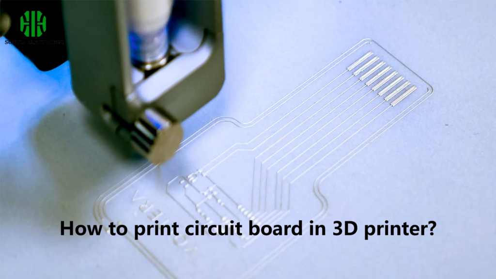
How to print circuit board in 3D printer?
- Design the PCB: Use PCB design software to create your circuit layout. Tools like Eagle, KiCAD, or Altium Designer can be used to design the schematic and board layout.
- Convert the Design for 3D Printing: The design must be exported in a format suitable for 3D printing, typically STL or OBJ. Some special software or plugins might be needed to convert standard PCB design files into 3D printable files.
- Upload the CAD file online and select materials: Many 3D printing services allow you to upload your CAD file online and select the materials for your PCB. This can provide an instant quote and ensure you choose the best materials for your project.
- Prepare the PCB printer: Load the printer with the appropriate materials (conducting and insulating). Make sure the printer is calibrated to handle the fine details of PCB tracks.
- Print the Base Layer: Start by printing the insulating base layer of the PCB. This layer forms the foundation of the circuit board.
- Print the Conductive Traces: Using a conductive filament or ink, print the circuit traces onto the base layer. The accuracy and resolution of your printer are crucial here to ensure the traces are well-defined and have good conductivity.
- Component Placement and Soldering: Once the printing is complete, components can be placed and soldered onto the board as usual. Some 3D printers with multiple heads can also place components during the printing process.
What materials, including conductive filament, are required to print a PCB with a 3D printer?
Conductive Filament or Ink: For the conductive traces, materials such as conductive PLA, graphene-infused filament, or specially formulated conductive inks are used. The choice of materials is crucial in the manufacturing process of 3D printed PCBs, as it affects the conductivity and durability of the final product.
Insulating Filament: Typically, a standard plastic filament like PLA or ABS is used for the base layer of the PCB.
| Material Type | Description | Availability |
|---|---|---|
| Conductive Filament or Ink | Used for printing circuit pathways | Widely available in specialty stores |
| Insulating Filament | To separate different electrical paths | Online, specialty electronics shops |
3D Printing Technologies for PCBs
Several 3D printing technologies are used to produce PCBs, each with its own set of advantages and applications.
- Fused Deposition Modeling (FDM): This is one of the most popular 3D printing technologies for producing PCBs. FDM involves extruding conductive filament through a heated nozzle to create the desired circuit pattern. The process is relatively simple and cost-effective, making it suitable for rapid prototyping and small-scale production. FDM is particularly useful for creating basic circuit boards with moderate complexity.
- Selective Laser Sintering (SLS): SLS is another advanced 3D printing technology used to produce PCBs. It involves using a laser to fuse together conductive particles, creating a solid circuit pattern. SLS offers higher resolution and better material properties compared to FDM, making it suitable for more complex and high-performance PCBs. This technology is ideal for applications that require precise and durable circuit boards.
- Multi-Jet Fusion (MJF): MJF is a cutting-edge 3D printing technology that combines inkjet printing and fusion to create PCBs. This method offers high resolution and accuracy, making it suitable for producing intricate and complex circuit designs. MJF can produce high-quality PCBs with excellent electrical properties, making it a preferred choice for advanced applications in consumer electronics and industrial control systems.
Each of these technologies has its own strengths, and the choice of technology depends on the specific requirements of the PCB design, including complexity, resolution, and material properties.
What are the advantages of using additive manufacturing to make PCBs?
- Rapid Prototyping: 3D printing allows for quick turnaround on PCB prototypes, enabling faster iterative development.
- Complexity and Customization: 3D printing allows for the creation of complex and non-traditional printed circuit board shapes, making it easier to customize each print.
- Reduction in Waste: Traditional etching of PCBs involves chemicals and produces waste; 3D printing can be more environmentally friendly by using only the necessary material.
What are the limitations of 3D printed PCBs compared to traditional PCBs?
- Conductivity: Conductive filaments and inks are typically less conductive than traditional copper, potentially affecting the performance in high-power or high-frequency applications.
- Resolution: The resolution of 3D printers, especially in laying down fine conductive traces, might not match the precision of traditional methods, impacting the functionality of highly detailed circuits.
- Durability and Reliability: 3D printed PCBs might not have the same durability or reliability as traditional PCBs, especially under thermal stress or in rugged environments.
| Feature | 3D Printed PCBs | Traditional PCBs |
|---|---|---|
| Complexity of Circuits | Limited | High |
| Production Time | Quick | Varies |
| Cost | Lower for prototypes | Economical at scale |
How long can the 3D printed PCB be used?
The lifespan of a 3D printed PCB can vary widely based on the materials used, the operating environment, and the electrical demands placed on the board. Typically, these PCBs are best suited for prototyping and low-stress applications. For critical or long-term applications, traditional PCBs might still be preferable due to their proven reliability and durability. In general, expect a 3D printed PCB to be a temporary solution unless specifically designed and tested for longer-term use.

