What is PCBA? The Complete Guide for Electronics Buyers
Leading paragraph:
Do you know PCBA controls every electronic device around you? Let me cut through the confusion for global buyers seeking reliable Chinese suppliers.
Snippet paragraph:
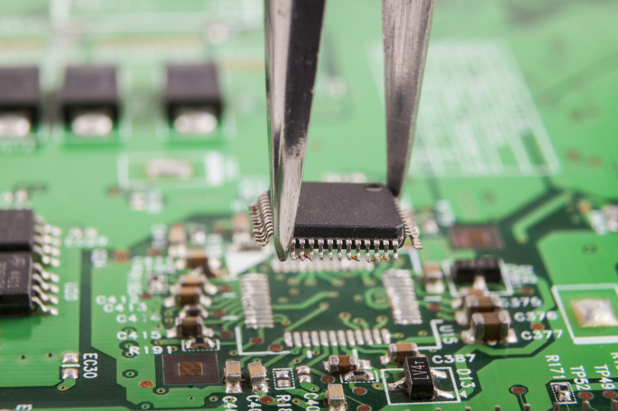
PCBA stands for Printed Circuit Board Assembly. It’s the final stage where electronic components are installed on a bare PCB. Finished PCBA boards power devices from medical equipment to smartphones.
g)
"PCB and PCBA manufacturing process")
Transition Paragraph:
Understanding PCBA details separates successful electronics projects from costly failures. Let’s answer key questions I’ve encountered from American buyers like you.
What is the Difference Between PCB and PCBA?
Leading paragraph:
Ordering the wrong product costs time and money. Let’s clarify this fundamental distinction.
Snippet paragraph:
A PCB (Printed Circuit Board) is the blank fiberglass board with copper traces. PCBA (Printed Circuit Board Assembly) is the functional board with all components soldered on.
0)
Dive deeper paragraph:
Three Critical Differences Every Buyer Must Verify
| Feature | PCB | PCBA |
|---|---|---|
| Stage of Production | Raw circuit board | Completed electronic module |
| Components Included | None – just copper pathways | All ICs, capacitors, resistors |
| Testing Requirements | Electrical conductivity only | Full functional testing |
At our Shenzhen factory, we see 37% of quality issues arise from buyers not specifying PCB vs PCBA needs. Always confirm:
- Required certifications (UL, ISO, etc.)
- Component sourcing responsibility
- Testing protocols (AOI, X-ray, functional)
"Many clients mistakenly think PCB orders include components. I recommend using PCBA contracts when you need ready-to-use boards." – Amy Loo, Production Manager
What is SMT and How Does It Relate to PCBA?
Leading paragraph:
The secret behind your iPhone’s motherboard lies in this manufacturing process.
Snippet paragraph:
SMT (Surface Mount Technology) is the standard method for attaching components to PCBs. It enables high-speed, precision PCBA production for modern electronics.
)
Dive deeper paragraph:
The SMT Process: Step-by-Step
-
Solder Paste Application
Our Yamaha machines apply paste with 0.01mm precision -
Component Placement
High-speed robots place 25,000 components/hour -
Reflow Soldering
Temperature-controlled ovens create permanent bonds
Key advantages over older through-hole technology:
- Space saving: Components on both board sides
- Cost efficiency: 68% faster assembly
- Reliability: Fewer manual soldering errors
Our 3 dedicated sample lines use Mitsubishi SMT equipment for prototypes. This allows 24-hour turnaround for urgent PCBA samples.
How Does Bare PCB Differ from Finished PCB?
Leading paragraph:
This isn’t wordplay – the distinction impacts your project timeline and costs.
Snippet paragraph:
"Bare PCB" refers to an unpopulated circuit board. "PCB" can sometimes mean either bare or assembled boards, while "PCBA" always means fully assembled.
)
Dive deeper paragraph:
When to Order Which Version?
| Scenario | Order Bare PCB | Order PCBA |
|---|---|---|
| In-house assembly capabilities | ✓ | ✗ |
| Small prototype batches | ✗ | ✓ (faster turnaround) |
| Strict quality control needs | ✗ (harder to verify) | ✓ (full testing) |
Most American clients now prefer full PCBA service. Last year, 82% of our export orders were PCBA rather than bare PCBs. Key reasons include:
- Reduced logistics costs (components come from our vetted suppliers)
- Single-point quality responsibility
- Faster time-to-market
Why is PCBA Critical in Mobile Devices?
Leading paragraph:
Your smartphone contains the most advanced PCBA engineering. Here’s what matters.
Snippet paragraph:
Mobile PCBA requires ultra-precise component placement and rigorous testing. Even 0.1mm errors can ruin compact device designs.
)
Dive deeper paragraph:
5 Mobile PCBA Requirements We Enforce
-
Micro Components
Handling 01005 package size (0.4mm x 0.2mm) -
Multilayer Boards
Up to 18-layer boards for space efficiency -
Flexible PCBAs
Using polyimide substrates for foldable phones -
Thermal Management
Special solder alloys preventing overheating -
Drop Testing
1,000+ drop simulations before approval
Our factory’s ISO-9001 certified mobile PCBA line serves major Chinese phone brands. We implement:
- Daily machine calibration
- 100% AOI (Automated Optical Inspection)
- Batch traceability system
Conclusion
PCBA transforms bare boards into functional electronics. Partner with suppliers who control the entire process. Need reliable PCBA? Email amy@southelectronicpcb.com for samples tested to your standards.


