
Custom 8-Layer PCB Manufacturing Services
Min trace 3/3 mil | ENIG / HASL | FR-4 & High-TG | AOI & E-Test
We manufacture high-precision 8-layer PCBs for industrial, IoT, and power electronics, with stable quality and consistent performance for repeat production.
8-Layer PCB Capabilities
Rigid PCB Process Capability
-
Layer Count
8 layers
-
PCB Dimensions
≤24*48inch(610*1220mm)
-
Materials Types
FR-4 | High Tg | Halogen-free | PTFE | Ceramic PCB | Metal substrate material
-
Material Brand
Lianmao|Shengyi| Taiyao| Nanya, Panasonic|Isola|Nelco|Rogers|Taconic|Arlon...
-
Board Thickness
0.2mm-8.0mm
-
Finish Treatment
Immersion Gold|Lead-free HASL|OSP|Immersion Tin|Immersion Silver|Thick Gold Plating|Silver Plating|Immersion Gold+OSP
-
Copper thickness
0.33 OZ-8 OZ
-
SolderMask Color
Green| Blue| Black|Yellow| Red|Purple| White...
-
Finish Treatment
Immersion Gold|Lead-free HASL|OSP|Immersion Tin|Immersion Silver|Thick Gold Plating|Silver Plating|Immersion Gold+OSP
Why Choose Us for 8-Layer PCB Manufacturing
We support engineers with reliable 8-layer PCB manufacturing,
from prototype builds to stable repeat production.
Every 8-layer PCB is reviewed by our engineers to verify stack-up, impedance control, and manufacturability before production.
We focus on consistent quality across batches, supporting both prototypes and long-term production.
Experienced in tight trace/space, controlled impedance, and multilayer lamination for complex designs.
Clear technical communication and fast response to support overseas engineering and purchasing teams.
Related Project We Had Done
8-Layer PCB for Industrial Control System
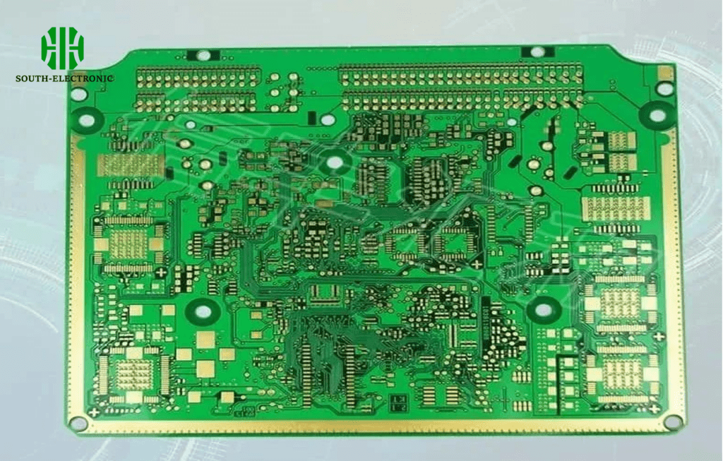
Application
Industrial Control
Key Specs
8-layer, controlled impedance
Challenge
Dense layout & signal integrity
Result
Stable performance in mass production
8-Layer PCB for Industrial Power Control
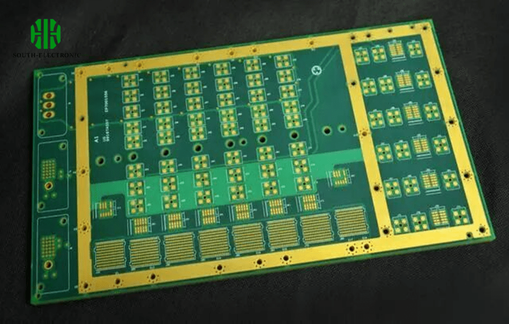
Application
Industrial Power Control
Key Specs
8-layer, heavy copper, controlled impedance
Challenge
High current handling with thermal management requirements
Result
Reliable operation under continuous load in mass production
8-Layer PCB for IoT Gateway Device
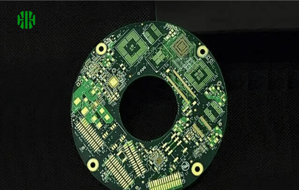
Application
IoT Gateway & Communication Device
Key Specs
8-layer, HDI structure, impedance controlled
Challenge
High-density layout with signal integrity for high-speed interfaces
Result
Stable signal performance and consistent quality across batches
Quality Control & Certifications for 8-Layer PCB Production
Common Questions
Most Popular Questions
What is the typical lead time for 8-layer PCB production?
Prototype lead time is typically 7–10 working days.
Mass production lead time depends on quantity and specifications.
Do you support controlled impedance for 8-layer PCBs?
Yes. We support impedance control and provide stack-up review and impedance calculation before production.
What materials are available for 8-layer PCBs?
Common materials include FR-4, High-TG FR-4, and other special materials upon request.
What quality control processes are applied to 8-layer PCBs?
All 8-layer PCBs undergo AOI inspection, electrical testing (E-Test), and process control throughout production.
What files are required to get an 8-layer PCB quotation?
Please provide Gerber files, PCB quantity, and any special requirements such as impedance control or material preference.
Send Us a Message
The more detailed you fill out, the faster we can move to the next step.

