
Introduce
In the rapidly evolving landscape of the electronics industry, digital printed circuit boards (PCBs) stand out as a cornerstone of modern electronic design and manufacturing. One of the most significant advantages of digital PCBs is their ability to support complex circuit designs within a compact layout. As devices become smaller and the demand for multifunctionality increases, digital PCBs enable the integration of a high number of components on a single board.

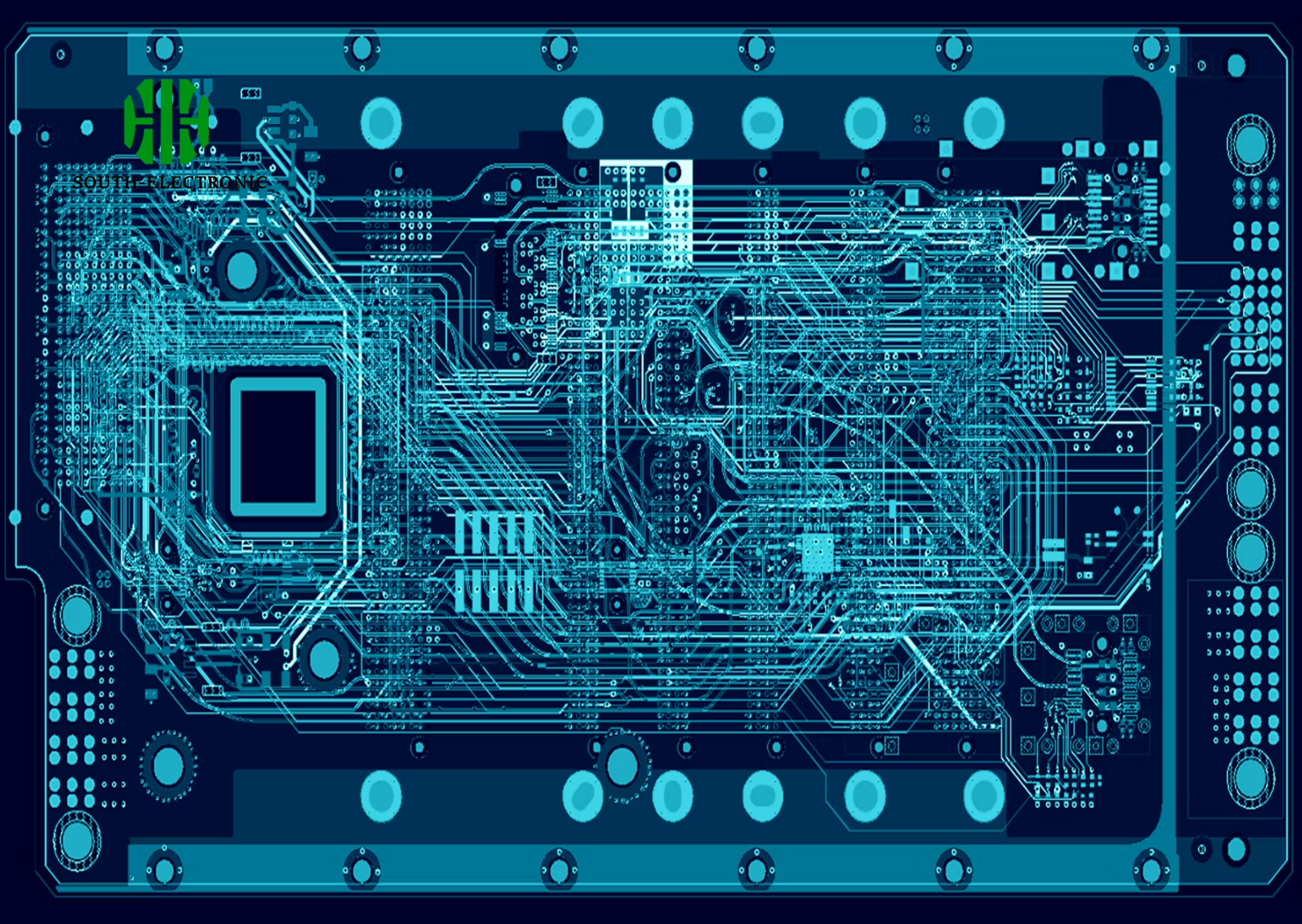
Typical Features of Digital PCBs
- Digital PCBs primarily deal with digital signals, where information is encoded in binary format (0s and 1s).
- Digital PCBs tend to support higher complexity and component density.
- Digital PCBs often incorporate sophisticated power management schemes to address the varying power demands of digital componen.
- One of the critical attributes of digital PCBs is their enhanced signal integrity and speed.
- Digital PCBs exhibit improved power efficiency, a paramount feature given the increasing emphasis on sustainability and energy conservation in electronics manufacturing.
- Digital PCBs, due to their high component density and power consumption, often require advanced thermal management solutions.
Digital PCBs Applications
Digital Printed Circuit Boards (PCBs) serve as the backbone for a multitude of electronic devices, enabling advancements across various sectors. The unique attributes of digital PCBs—such as high component density, enhanced signal integrity, and power efficiency—make them ideal for a wide range of applications. Usually used in network communications, radios, electronic equipment, medical industry, automotive industry and aerospace, etc.

Considerations for Designing Digital PCBs
- Reducing noise emitted from the power source and mitigating switch noise arising from ongoing power supply operations.
- Decreasing interference among signal paths.
- Diminishing the impact of ground bounce effects.
- Taking into account the proper termination of signal lines.
- Guaranteeing correct impedance alignment.
- Selecting the optimal materials, including FR-4, High Tg FR-4, Polyimide, among others.
Conclusion
The typical features of digital PCBs reflect the complex requirements of modern electronic devices, from compactness and efficiency to performance and reliability. As technology advances, these features evolve, pushing the boundaries of PCB design and manufacturing. Understanding these characteristics is crucial for anyone involved in the creation, application, or study of digital electronics, providing the foundation for the next generation of innovations.


