Top 4 Layer PCB Suppliers
South-Electronic
With South-Electronic, you get unmatched quality and consistency in your electronic projects. Our 4 layer PCBs elevate your devices’ performance through exceptional electrical performance and mechanical resilience. Partner with us to achieve excellence and success in your industry.
Why Choose South-Electronic?
-
Flexibility in Ordering:
Enjoy the flexibility of ordering from MOQ 1pc, tailored to your specific needs.
-
Experienced Team:
Leverage over a decade of industry experience from our team members.
-
Strict Quality Control:
With UL, CE, IATF16949, ISO13485, every PCB is made with strict quality control.
-
Comprehensive Service:
Efficient production and operations ensure quick turnaround times.
-
Fast Delivery:
Efficient production and operations ensure quick turnaround times.
-
Guaranteed Satisfaction:
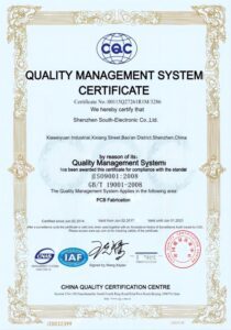
We are an ISO9001 certified factory committed to quality and clear communication.
-
Tailored to Your Automotive Needs:
We recognize that each automotive project is unique. That's why we meticulously develop specifications that are customized to guarantee your project's success.
-
Wide Range of Options:
From flex circuits to thermal management PCBs, our extensive selection ensures we have the perfect solution for your automotive application.
-
Optimized Performance:
Using state-of-the-art engineering techniques, we enhance the PCB's performance to meet your exact specifications, delivering efficient and reliable results.
-
Balanced Durability:
We adjust material properties to balance durability and performance, ensuring a long lifespan without sacrificing functionality.
Related Project We had Done
Customer Reviews
Common Questions
Most Popular Questions
Send us a message
The more detailed you fill out, the faster we can move to the next step.










The Complete Guide For 4 Layer PCB
Cahpter 1
Introduction to 4 Layer PCBs
Definition and Basic Structure
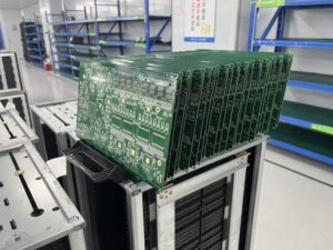
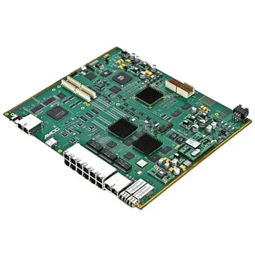
A 4 layer PCB (Printed Circuit Board) is a type of multilayer PCB that consists of four layers of conductive copper separated by insulating layers. The layers are stacked together in the following order:
- Top Layer (Signal Layer): This is the first layer where most of the surface-mounted components are placed.
- Inner Layer 1 (Power Plane): This layer is typically used to distribute power to various components on the board, ensuring consistent voltage levels and reducing power supply noise.
- Inner Layer 2 (Ground Plane): This layer is dedicated to ground connections, providing a common return path for current and minimizing electromagnetic interference (EMI).
- Bottom Layer (Signal Layer): Similar to the top layer, this layer is used for routing signals and placing components.
The layers are bonded together with insulating materials, typically made of FR4, which is a flame-resistant fiberglass epoxy laminate. The structure of a 4 layer PCB allows for more complex designs, higher component density, and improved performance compared to single-layer and double-layer PCBs.
Importance in Modern Electronics
4 layer PCBs are crucial in modern electronics due to their ability to support high-speed, high-density, and high-performance designs. Here are some key reasons why 4 layer PCBs are essential:
- Enhanced Signal Integrity: The additional layers provide dedicated planes for power and ground, which helps in reducing noise and crosstalk between signal traces. This is especially important in high-frequency applications where signal integrity is critical.
- Increased Routing Density: With four layers, designers have more routing space, allowing for more complex circuits without compromising on performance. This is beneficial in compact devices where space is at a premium.
- Improved Thermal Management: The multiple layers can dissipate heat more effectively, reducing the risk of overheating and improving the reliability and lifespan of the electronic components.
- Better Electromagnetic Compatibility (EMC): The use of ground planes helps in shielding sensitive components and reducing electromagnetic interference, which is vital for meeting regulatory standards in various industries.
Overview of Applications and Industries
4 layer PCBs are used across a wide range of applications and industries due to their versatility and advanced capabilities. Here are some notable applications and industries:
Telecommunications: In telecommunications equipment, 4 layer PCBs are used in devices such as routers, switches, and modems, where they help in managing high-speed data transfer and complex signal processing.
Medical Devices: Precision and reliability are paramount in medical devices. 4 layer PCBs are used in diagnostic equipment, imaging systems, and patient monitoring devices to ensure accurate performance and safety.
Industrial Controls: In industrial automation and control systems, 4 layer PCBs are used in programmable logic controllers (PLCs), motor drives, and sensors, providing robust and reliable operation in harsh environments.
Consumer Electronics: Many modern consumer electronics, such as smartphones, tablets, and gaming consoles, rely on 4 layer PCBs to handle their advanced features and compact designs.
Automotive Applications: The automotive industry uses 4 layer PCBs in various electronic control units (ECUs), infotainment systems, and advanced driver-assistance systems (ADAS) to ensure performance and reliability under demanding conditions.
Aerospace and Defense: In aerospace and defense applications, 4 layer PCBs are used in communication systems, navigation equipment, and control systems, where high reliability and precision are essential.
In conclusion, 4 layer PCBs are a fundamental component in the development of modern electronic devices, offering enhanced performance, reliability, and versatility. Their ability to support complex designs and high-speed applications makes them indispensable in various high-tech industries. As technology continues to advance, the demand for 4 layer PCBs is expected to grow, driving innovation and improvements in electronic design and manufacturing.
Cahpter 2
Advantages of 4 Layer PCB
Improved Signal Integrity
Signal integrity is a critical factor in the design of modern electronic devices, especially those operating at high frequencies. The design and structure of 4 layer PCBs significantly enhance signal integrity through the following means:
Dedicated Power and Ground Planes: In a 4 layer PCB, one of the inner layers is typically dedicated to power distribution, while another is reserved for ground. This configuration provides a stable reference voltage and minimizes voltage fluctuations, which can cause noise and signal distortion.
Reduced Crosstalk: By separating signal layers with ground planes, 4 layer PCBs help to minimize crosstalk between adjacent traces. Crosstalk occurs when signals in one trace induce unwanted voltages in neighboring traces, leading to signal interference and degradation.
Controlled Impedance: 4 layer PCBs allow for precise control over the impedance of signal traces. Controlled impedance is essential for high-speed digital and RF circuits, ensuring that signals propagate with minimal reflection and distortion.
Lower Signal Path Inductance and Capacitance: The additional layers in a 4 layer PCB reduce the inductance and capacitance of signal paths, enabling faster signal transmission and reducing the likelihood of signal loss and distortion.
Enhanced Electromagnetic Compatibility (EMC)
Electromagnetic Compatibility (EMC) refers to the ability of electronic devices to operate without interfering with other electronic devices and without being affected by external electromagnetic interference (EMI). 4 layer PCBs offer several advantages in terms of EMC:
Effective Ground Plane Shielding: The ground plane in a 4 layer PCB acts as a shield, protecting sensitive components and traces from external EMI. This shielding helps to prevent electromagnetic emissions from the PCB itself, reducing the risk of interference with other devices.
Minimized Loop Area: By placing power and ground planes in close proximity, 4 layer PCBs reduce the loop area for current paths. Smaller loop areas result in lower radiated emissions and improved immunity to external noise.
Better Signal Return Paths: The dedicated ground plane provides a low-impedance return path for signals, minimizing the potential for EMI and ensuring that signal currents return to their sources with minimal disruption.
Enhanced Filtering and Decoupling: The layered structure of 4 layer PCBs allows for the strategic placement of decoupling capacitors and other filtering components. These components help to suppress high-frequency noise and stabilize power delivery, further enhancing EMC performance.
Increased Routing Density and Functionality
4 layer PCBs offer significantly higher routing density and functionality compared to single-layer and double-layer PCBs. This increased density provides several benefits:
Complex Circuit Design: The additional layers in a 4 layer PCB allow for more complex circuit designs, accommodating a greater number of components and interconnections. This capability is essential for advanced electronic devices with multiple functions and features.
Optimized Trace Routing: With more layers available for routing, designers can optimize the placement and routing of signal traces. This optimization reduces the need for long, convoluted trace paths, which can introduce delays and signal degradation.
Improved Component Placement: The increased routing density enables more efficient use of the PCB surface area, allowing for better component placement and reduced board size. This efficiency is particularly important in compact electronic devices where space is at a premium.
Support for High-Pin-Count Components: 4 layer PCBs can accommodate high-pin-count components, such as microprocessors and FPGAs, which require extensive interconnections. The additional layers provide the necessary routing space to connect all pins without overcrowding the board.
Space and Weight Reduction in Compact Designs
In modern electronic design, space and weight are critical considerations, especially for portable and wearable devices. 4 layer PCBs contribute to space and weight reduction through the following means:
Compact Form Factor: The increased routing density of 4 layer PCBs allows for a more compact form factor. By utilizing multiple layers for routing, designers can reduce the overall dimensions of the PCB while maintaining functionality and performance.
Integration of Multiple Functions: 4 layer PCBs enable the integration of multiple functions and components on a single board. This integration reduces the need for additional boards and interconnections, resulting in a lighter and more compact overall design.
Reduced Layer Stack Thickness: Despite having more layers, advanced manufacturing techniques allow for the production of 4 layer PCBs with relatively thin layer stacks. This reduction in thickness helps to minimize the weight of the PCB.
Enhanced Mechanical Stability: The layered structure of 4 layer PCBs provides enhanced mechanical stability, allowing for the use of thinner and lighter materials without compromising durability. This stability is particularly important in portable and wearable devices that are subjected to physical stress.
In conclusion, the advantages of 4 layer PCBs make them indispensable in the design and manufacturing of modern electronic devices. Improved signal integrity, enhanced electromagnetic compatibility, increased routing density and functionality, and space and weight reduction are critical factors that drive the adoption of 4 layer PCBs across various industries. As electronic devices continue to evolve, the demand for advanced PCB solutions like 4 layer PCBs is expected to grow, fostering innovation and advancements in electronic design and manufacturing.

Cahpter 3
Materials and Construction of 4 Layer PCB
Common Materials Used
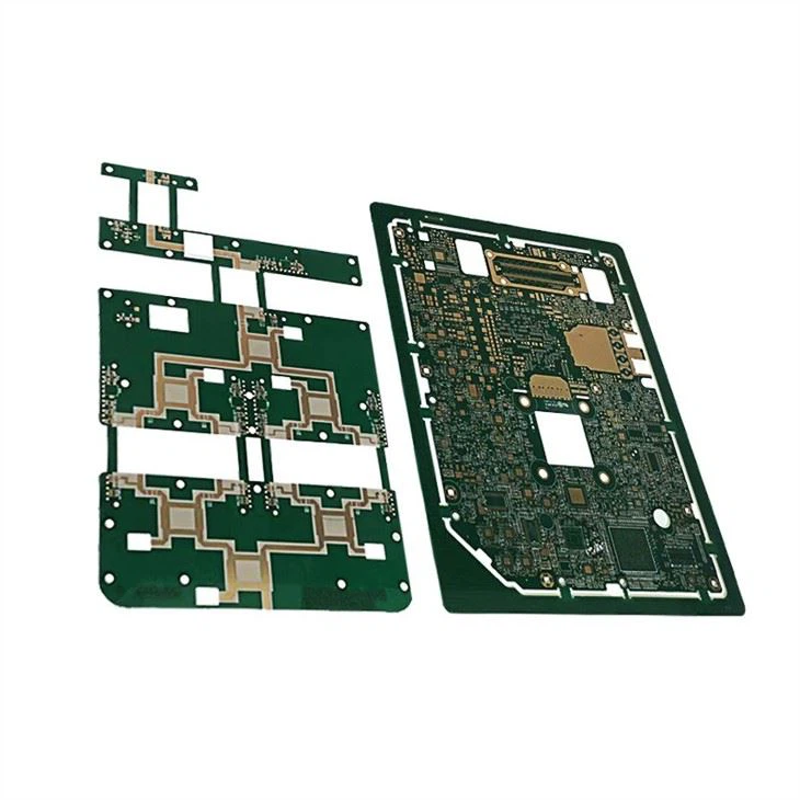
The choice of materials in a 4 layer PCB significantly impacts its performance, reliability, and suitability for various applications. Here are the common materials used in the construction of 4 layer PCBs:
FR4 (Flame Retardant 4)
- Properties: FR4 is a glass-reinforced epoxy laminate known for its excellent strength-to-weight ratio, mechanical stability, and insulating properties. It is flame retardant, providing safety and durability.
- Applications: FR4 is the most widely used material in standard PCBs due to its balance of performance, cost, and ease of processing.
High TG (High Glass Transition Temperature) Materials
- Properties: High TG materials can withstand higher temperatures before transitioning from a rigid state to a more pliable one. They provide enhanced thermal performance and stability.
- Applications: These materials are used in applications where the PCB will be exposed to elevated temperatures, such as in automotive, aerospace, and industrial electronics.
Flexible Materials
- Properties: Flexible materials, such as polyimide, offer the ability to bend and flex without compromising electrical performance. They provide excellent thermal stability and chemical resistance.
- Applications: Flexible PCBs are used in dynamic applications where the PCB needs to conform to different shapes, such as in wearable devices, medical equipment, and foldable electronics.
Other Specialized Materials
- Properties: Other materials like Rogers, Teflon, and metal core substrates are used for specific applications requiring unique properties such as high-frequency performance, low dielectric loss, or enhanced thermal dissipation.
- Applications: These specialized materials are used in RF and microwave circuits, power electronics, and other high-performance applications.
Detailed Layer Composition
The construction of a 4 layer PCB involves a meticulous layering process, with each layer serving a specific function:
Top Layer (Signal Layer)
- Function: The top layer is used for routing signal traces and placing surface-mounted components. It typically handles high-speed signals and connections to external interfaces.
- Materials: Copper foil laminated onto the substrate, coated with a solder mask and silkscreen for component placement and identification.
Inner Layer 1 (Power Plane)
- Function: This layer distributes power to various components, ensuring stable and consistent voltage levels across the PCB. It helps in reducing power supply noise and improving overall performance.
- Materials: Copper plane, often with thicker copper for higher current carrying capacity, laminated with an insulating layer of FR4 or other suitable material.
Inner Layer 2 (Ground Plane)
- Function: The ground plane provides a common return path for current and minimizes electromagnetic interference (EMI). It also serves as a reference plane for signal traces.
- Materials: Copper plane, similar to the power plane, laminated with an insulating layer to separate it from other conductive layers.
Bottom Layer (Signal Layer)
- Function: The bottom layer is used for additional signal routing and component placement. It often handles less critical or slower speed signals compared to the top layer.
- Materials: Similar to the top layer, with copper foil, solder mask, and silkscreen.
The layers are bonded together with pre-preg (pre-impregnated) materials, which are layers of fiberglass cloth impregnated with resin. The pre-preg layers act as adhesive and insulators between the conductive copper layers.
Manufacturing Process Overview
The manufacturing of a 4 layer PCB involves several precise and controlled steps to ensure high quality and performance:
Design and Layout
- Step: The PCB design is created using specialized software tools. The layout includes the placement of components, routing of signal traces, and definition of power and ground planes.
- Output: Gerber files, which contain the detailed design data for each layer of the PCB.
Material Preparation
- Step: The raw materials, including copper-clad laminates and pre-preg sheets, are prepared. The copper-clad laminates are typically made of FR4 or other chosen materials.
- Output: Laminates and pre-preg sheets cut to the required size.
Inner Layer Imaging and Etching
- Step: The inner layers (power and ground planes) are imaged using a photoresist process, where a light-sensitive film is applied, exposed to UV light, and developed to create the desired pattern. The unexposed areas are then etched away to leave the copper patterns.
- Output: Completed inner layers with etched copper patterns.
Lamination
- Step: The etched inner layers are stacked with pre-preg sheets and outer copper layers, then pressed together under heat and pressure in a laminating press. This process bonds the layers into a single solid board.
- Output: Laminated 4 layer PCB, ready for further processing.
Drilling
- Step: Holes are drilled into the PCB to create vias (vertical interconnect access) and mounting holes. These vias connect different layers electrically and are crucial for the PCB’s functionality.
- Output: Drilled PCB with precise hole placement.
Plating and Outer Layer Imaging
- Step: The drilled holes are plated with copper to create electrical connections between layers. The outer layers are then imaged and etched using a similar process as the inner layers.
- Output: PCBs with fully patterned and plated outer layers.
Solder Mask Application
- Step: A solder mask is applied to protect the copper traces and prevent solder bridging during component assembly. The solder mask also enhances the board’s durability and electrical insulation.
- Output: PCB with solder mask applied.
Silkscreen Printing
- Step: The silkscreen layer is printed with component identifiers, logos, and other necessary markings to aid in assembly and inspection.
- Output: PCB with silkscreen markings.
Surface Finish
- Step: A surface finish is applied to the exposed copper areas to prevent oxidation and improve solderability. Common finishes include HASL (Hot Air Solder Leveling), ENIG (Electroless Nickel Immersion Gold), and OSP (Organic Solderability Preservatives).
- Output: PCB with surface finish applied.
Testing and Inspection
- Step: The completed PCB undergoes electrical testing, including continuity and insulation tests, to ensure there are no shorts or open circuits. Visual inspections are also conducted to verify the quality and accuracy of the board.
- Output: Tested and inspected PCB, ready for assembly.
In conclusion, the construction of a 4 layer PCB involves a series of well-defined steps and the use of high-quality materials to ensure optimal performance and reliability. Each stage of the manufacturing process is critical to producing a PCB that meets the stringent requirements of modern electronic applications.
Cahpter 4
Design Considerations for 4 Layer PCB
Key Design Principles
Designing a 4 layer PCB requires careful attention to various principles to ensure optimal performance, reliability, and manufacturability. Key design principles include:
Layer Stackup Configuration
- The layer stackup defines the arrangement of signal, power, and ground layers. A typical 4 layer PCB stackup might consist of:
- Top Layer (Signal)
- Inner Layer 1 (Ground Plane)
- Inner Layer 2 (Power Plane)
- Bottom Layer (Signal)
- Proper stackup helps in minimizing electromagnetic interference (EMI) and improving signal integrity.
- The layer stackup defines the arrangement of signal, power, and ground layers. A typical 4 layer PCB stackup might consist of:
Impedance Control
- Impedance control is critical for high-speed signal transmission. Trace widths, spacing, and the dielectric properties of the materials must be carefully calculated to maintain consistent impedance.
- Controlled impedance ensures minimal signal reflection and distortion.
Power Distribution Network (PDN) Design
- A well-designed PDN minimizes noise and ensures stable power delivery to all components.
- Decoupling capacitors should be strategically placed near power pins to filter out noise and provide a stable voltage supply.
Grounding
- A solid ground plane is essential for signal integrity and EMI control. It provides a low-impedance return path for signals, reducing noise and crosstalk.
- Ground planes should be continuous and as uninterrupted as possible.
Thermal Management
- Efficient thermal management is necessary to prevent overheating and ensure the longevity of the components.
- Heat sinks, thermal vias, and proper component placement help in dissipating heat.
Layout Tips for Signal Integrity and Power Distribution
Signal Layer Routing
- High-speed signal traces should be routed on the top and bottom layers, while the inner layers are reserved for power and ground planes.
- Differential pairs should be routed together with controlled spacing to maintain impedance and minimize noise.
- Avoid 90-degree bends in traces as they can cause impedance discontinuities; use 45-degree bends or rounded corners instead.
Via Placement
- Use vias to connect different layers, but minimize their use to reduce inductance and signal degradation.
- Ensure vias are properly placed to avoid unnecessary stubs and impedance mismatches.
Power Plane Design
- The power plane should be designed to distribute power uniformly across the PCB.
- Use multiple vias to connect the power plane to the top and bottom layers, reducing resistance and inductance.
Decoupling Capacitors
- Place decoupling capacitors close to the power pins of ICs to filter out noise.
- Use a combination of capacitors with different values to filter a wide range of frequencies.
Minimize Crosstalk
- Maintain adequate spacing between signal traces to reduce crosstalk.
- Use ground traces or planes between high-speed signal traces as shields.
Return Path Considerations
- Ensure a continuous and low-impedance return path for all signal traces.
- Avoid routing high-speed signals over splits in the ground plane, as this can cause signal integrity issues.
Thermal Management Strategies
Component Placement
- Place heat-generating components, such as power regulators and processors, in areas with good airflow.
- Distribute heat-generating components evenly across the PCB to avoid hot spots.
Thermal Vias
- Use thermal vias to transfer heat from the top layer to the bottom layer or to internal heat-dissipating layers.
- Fill thermal vias with conductive material to enhance heat transfer.
Heat Sinks and Thermal Pads
- Attach heat sinks to high-power components to dissipate heat effectively.
- Use thermal pads to improve heat transfer between components and the PCB.
Copper Pours
- Utilize large copper areas (copper pours) connected to ground or power planes to dissipate heat.
- Ensure copper pours are thermally connected to heat-generating components.
Thermal Simulation
- Perform thermal simulations to predict and analyze the thermal performance of the PCB design.
- Adjust the design based on simulation results to ensure adequate thermal management.
Software Tools for Design and Simulation
PCB Design Software
- Altium Designer: A comprehensive PCB design tool that offers advanced routing, simulation, and analysis features.
- Cadence Allegro: Known for its high-performance design capabilities and extensive library support.
- EAGLE: A popular tool for both hobbyists and professionals, offering schematic capture and PCB layout.
Simulation Tools
- HyperLynx: Provides signal integrity, power integrity, and thermal analysis to ensure robust PCB designs.
- Ansys HFSS: A 3D electromagnetic simulation software for analyzing high-frequency components and PCB designs.
- SPICE: Used for circuit simulation, allowing designers to analyze the behavior of their circuits before physical prototyping.
Thermal Analysis Tools
- Flotherm: A thermal simulation tool that helps in analyzing and optimizing thermal performance.
- Ansys Icepak: Provides comprehensive thermal management solutions for electronic designs, including PCBs.
Design Rule Check (DRC) Tools
- DRC in Altium Designer: Ensures that the PCB design complies with manufacturing capabilities and design standards.
- DRC in Cadence Allegro: Validates design rules and constraints to prevent errors during manufacturing.
In conclusion, designing a 4 layer PCB involves careful consideration of various principles, from layer stackup and impedance control to power distribution and thermal management. Utilizing advanced design and simulation tools can help in creating high-performance, reliable PCBs that meet the stringent requirements of modern electronic applications. By adhering to these design considerations, engineers can ensure their 4 layer PCB designs are optimized for signal integrity, power distribution, and thermal performance, ultimately leading to successful and efficient electronic products.
Cahpter 5

Applications of 4 Layer PCB
Telecommunications
In the telecommunications industry, 4 layer PCBs play a critical role in the development and operation of advanced communication systems. Their robust design and high signal integrity make them ideal for a range of applications:
Network Equipment
- Routers and Switches: 4 layer PCBs are used in routers and switches, which require high-speed data transmission and reliable performance. The additional layers provide improved signal integrity and reduce crosstalk, ensuring efficient data handling.
- Modems: Modems for both consumer and enterprise applications benefit from the enhanced capabilities of 4 layer PCBs, which support complex circuitry and high-frequency signals.
Wireless Communication Devices
- Base Stations: Telecommunications base stations rely on 4 layer PCBs for their ability to handle high power and complex signal processing. These PCBs ensure stable and efficient operation in various environmental conditions.
- Antennas: Advanced antenna systems for mobile networks use 4 layer PCBs to support high-frequency signals and maintain signal integrity over long distances.
Optical Communication
- Fiber Optic Transceivers: 4 layer PCBs are used in fiber optic transceivers to manage the high-speed optical signals and convert them into electrical signals with minimal loss and interference.
- Optical Network Units (ONUs): ONUs, which connect to fiber optic networks, leverage the high-density routing capabilities of 4 layer PCBs for efficient data transmission and reception.
Medical Devices
In the medical field, the reliability and precision of 4 layer PCBs are indispensable. They are used in a variety of critical applications where performance and safety are paramount:
Diagnostic Equipment
- MRI Machines: 4 layer PCBs in MRI machines ensure accurate signal processing and imaging, which are crucial for precise diagnostics.
- CT Scanners: These scanners use 4 layer PCBs to handle the complex data acquisition and processing needed for detailed cross-sectional imaging.
Patient Monitoring Systems
- Electrocardiograms (ECGs): 4 layer PCBs provide the necessary signal integrity and reliability for continuous monitoring of a patient’s heart activity.
- Blood Glucose Monitors: Portable blood glucose monitors use 4 layer PCBs to maintain accuracy and reliability in readings, which are vital for patient health management.
Therapeutic Devices
- Infusion Pumps: 4 layer PCBs ensure the precise control and delivery of medication in infusion pumps, which are critical for patient treatment.
- Pacemakers: Implantable pacemakers use 4 layer PCBs for their compact size and reliable performance, ensuring consistent heart rate regulation.
Industrial Controls
Industrial control systems demand high reliability and robust performance, both of which are provided by 4 layer PCBs. These PCBs are used in various industrial applications to enhance efficiency and control:
Programmable Logic Controllers (PLCs)
- Process Automation: 4 layer PCBs in PLCs handle complex control algorithms and signal processing, ensuring precise automation of industrial processes.
- Machine Control: PLCs equipped with 4 layer PCBs provide reliable control for machinery, improving operational efficiency and safety.
Motor Drives
- Variable Frequency Drives (VFDs): VFDs use 4 layer PCBs to manage motor speed and torque with high precision, enhancing energy efficiency and performance in industrial applications.
- Servo Drives: These drives rely on 4 layer PCBs for accurate control of motor position and speed, essential for applications requiring high precision.
Sensors and Actuators
- Environmental Sensors: 4 layer PCBs in environmental sensors ensure reliable data collection and processing, which is crucial for monitoring and control in industrial settings.
- Robotic Actuators: Robotic systems use 4 layer PCBs to handle the complex control and feedback mechanisms required for precise movement and operation.
Consumer Electronics
The consumer electronics industry is driven by innovation and miniaturization, making 4 layer PCBs an essential component in a wide range of products:
Smartphones and Tablets
- High Performance: 4 layer PCBs provide the necessary routing density and signal integrity for the advanced functionality of modern smartphones and tablets.
- Compact Design: The ability to stack multiple layers allows for more components to be placed in a smaller area, supporting the sleek designs of these devices.
Wearable Devices
- Smartwatches: Smartwatches use 4 layer PCBs to integrate multiple functions such as fitness tracking, notifications, and wireless communication into a compact form factor.
- Fitness Trackers: These devices rely on 4 layer PCBs for their advanced sensors and connectivity features, ensuring accurate tracking and data synchronization.
Home Automation
- Smart Home Hubs: 4 layer PCBs in smart home hubs provide the necessary connectivity and processing power to manage various home automation devices.
- Smart Appliances: Smart appliances, such as refrigerators and washing machines, use 4 layer PCBs to support advanced features like remote control and energy management.
Automotive Applications
In the automotive industry, the demand for electronic systems that enhance safety, performance, and comfort has led to the widespread use of 4 layer PCBs:
Advanced Driver Assistance Systems (ADAS)
- Safety Features: ADAS systems, including lane departure warning and adaptive cruise control, rely on 4 layer PCBs for processing data from sensors and cameras, ensuring timely and accurate responses.
- Autonomous Driving: Autonomous vehicles use 4 layer PCBs to handle the complex processing required for navigation and decision-making, integrating data from multiple sensors and systems.
Infotainment Systems
- Multimedia: 4 layer PCBs in automotive infotainment systems support high-speed data processing for multimedia applications, providing seamless entertainment and information to passengers.
- Connectivity: These systems also leverage 4 layer PCBs for advanced connectivity features, including Bluetooth, Wi-Fi, and GPS.
Engine Control Units (ECUs)
- Performance Optimization: ECUs use 4 layer PCBs to manage engine performance, fuel efficiency, and emissions, ensuring compliance with regulatory standards and enhancing vehicle performance.
- Reliability: The robust design of 4 layer PCBs ensures reliable operation in the harsh automotive environment, withstanding temperature fluctuations and vibrations.
Battery Management Systems (BMS)
- Electric Vehicles (EVs): In EVs, 4 layer PCBs in BMS units monitor and manage battery health, ensuring optimal performance and longevity of the battery pack.
- Hybrid Vehicles: Hybrid vehicles also use BMS with 4 layer PCBs to manage the interaction between the internal combustion engine and the electric motor, optimizing efficiency.
In conclusion, 4 layer PCBs are integral to the advancement and functionality of numerous industries. Their ability to support complex circuitry, high-speed signals, and robust performance makes them indispensable in telecommunications, medical devices, industrial controls, consumer electronics, and automotive applications. As technology continues to evolve, the role of 4 layer PCBs in driving innovation and enhancing the capabilities of electronic systems will only grow, making them a cornerstone of modern electronic design and manufacturing.
Cahpter 6
Quality Control and Standards for 4 Layer PCB
Industry Standards and Certifications
Ensuring the quality and reliability of 4 layer PCBs involves adhering to industry standards and obtaining relevant certifications. These standards and certifications are designed to ensure that PCBs meet specific performance, safety, and reliability criteria.
ISO9001
- Overview: ISO9001 is an international standard for quality management systems (QMS). It specifies requirements for a QMS that can enhance customer satisfaction through consistent product quality and continual improvement processes.
- Application: In PCB manufacturing, ISO9001 certification ensures that the manufacturer has established and follows a rigorous quality management system, covering everything from raw material procurement to final product delivery.
UL (Underwriters Laboratories)
- Overview: UL certification indicates that a product has been tested and meets stringent safety standards. For PCBs, UL certification typically involves testing for flammability, electrical performance, and overall safety.
- Application: 4 layer PCBs with UL certification provide assurance to customers that the boards are safe for use in various applications, particularly those requiring high reliability and safety, such as medical devices and automotive systems.
CE (Conformité Européenne)
- Overview: The CE mark signifies that a product complies with the essential health, safety, and environmental protection requirements of the European Economic Area (EEA). It is mandatory for products sold within the EEA.
- Application: CE certification for PCBs involves testing for electromagnetic compatibility (EMC) and low voltage directives, ensuring that the boards do not cause or are not susceptible to electromagnetic interference.
IATF 16949
- Overview: IATF 16949 is a global standard for automotive quality management systems. It aligns with ISO9001 but includes additional requirements specific to the automotive industry.
- Application: PCBs manufactured under IATF 16949 certification meet the stringent quality and reliability requirements of the automotive industry, ensuring their suitability for use in critical automotive applications.
ISO13485
- Overview: ISO13485 is an international standard for quality management systems specific to the medical device industry. It ensures that medical devices consistently meet customer and regulatory requirements.
- Application: 4 layer PCBs used in medical devices must comply with ISO13485 to ensure they meet the strict safety and reliability standards required in the healthcare industry.
Quality Assurance Processes
Quality assurance (QA) in PCB manufacturing involves systematic processes to ensure that every board meets the required specifications and performance standards. These processes include:
Incoming Material Inspection
- Overview: QA starts with the inspection of incoming raw materials, such as copper-clad laminates, solder masks, and other components. This step ensures that only high-quality materials are used in the manufacturing process.
- Application: Materials are checked for conformity with specified standards, and any defects or inconsistencies are identified and addressed before production begins.
Process Control
- Overview: During production, process control measures are implemented to monitor and control each stage of manufacturing. This includes etching, drilling, plating, and lamination processes.
- Application: Real-time monitoring and control systems are used to detect and correct any deviations from the set parameters, ensuring consistent quality throughout the production process.
In-Process Inspections
- Overview: Regular inspections are conducted at various stages of production to identify and rectify any defects early in the process. These inspections include visual checks, automated optical inspection (AOI), and electrical testing.
- Application: In-process inspections help to maintain high-quality standards and reduce the risk of defects in the final product.
Final Inspection and Testing
- Overview: Before the PCBs are shipped to customers, a final inspection and testing phase is conducted to ensure they meet all specified requirements. This includes thorough visual inspections and electrical tests.
- Application: The final inspection ensures that the PCBs are free from defects and fully functional, providing confidence in their reliability and performance.
Testing Methods and Reliability Assessments
Testing and reliability assessments are critical to ensuring that 4 layer PCBs perform as expected under various conditions. These methods include:
Electrical Testing
- Overview: Electrical testing involves checking the continuity and insulation resistance of the PCB to ensure that all connections are intact and there are no shorts or opens.
- Application: Automated test equipment (ATE) is used to perform these tests, which verify that the PCB functions correctly and meets the electrical specifications.
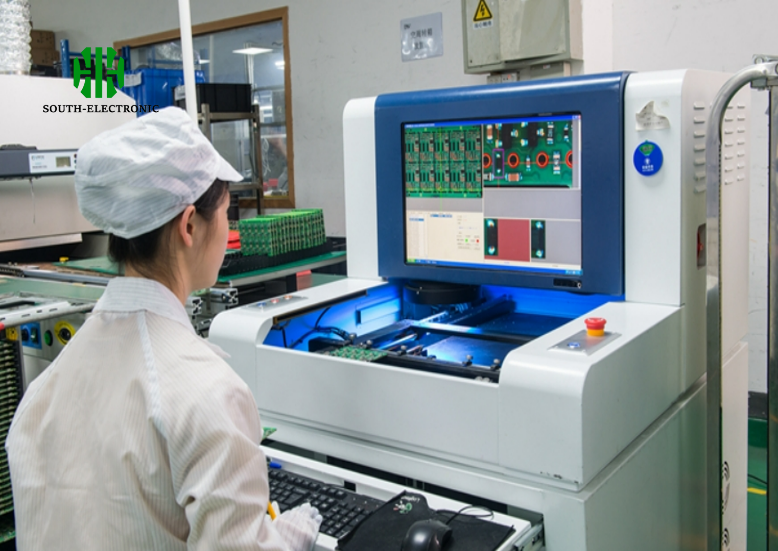
Automated Optical Inspection (AOI)
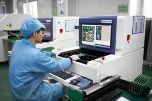
- Overview: AOI uses high-resolution cameras to inspect the PCB for defects such as missing components, incorrect placements, and soldering issues.
- Application: AOI is an essential part of the QA process, providing a non-contact method to quickly and accurately identify visual defects.
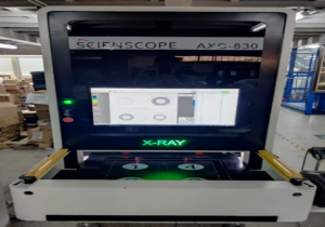
X-Ray Inspection
- Overview: X-ray inspection is used to examine the internal structure of the PCB, including the quality of solder joints, hidden connections, and internal layers.
- Application: This method is particularly useful for inspecting complex multilayer PCBs where visual inspection alone is insufficient.
Thermal Cycling Testing
- Overview: Thermal cycling tests involve exposing the PCB to repeated cycles of high and low temperatures to assess its thermal performance and reliability.
- Application: This testing method helps to identify potential issues related to thermal expansion and contraction, ensuring the PCB can withstand harsh environmental conditions.
Vibration Testing
- Overview: Vibration testing subjects the PCB to mechanical vibrations to simulate the conditions it might experience during transportation and operation.
- Application: This testing ensures that the PCB maintains its integrity and functionality under mechanical stress.
Environmental Testing
- Overview: Environmental testing evaluates the PCB’s performance under various environmental conditions, such as humidity, temperature, and corrosive atmospheres.
- Application: These tests help to ensure that the PCB can operate reliably in different environments, making it suitable for a wide range of applications.
Reliability Assessments
- Overview: Reliability assessments involve long-term testing and analysis to predict the lifespan and performance of the PCB under normal and extreme conditions.
- Application: Accelerated life testing (ALT) and highly accelerated life testing (HALT) are used to identify potential failure modes and improve the overall reliability of the PCB design.
In conclusion, quality control and adherence to industry standards are essential in the manufacturing of 4 layer PCBs. Through rigorous quality assurance processes and comprehensive testing methods, manufacturers can ensure that their PCBs meet the highest standards of performance, reliability, and safety. These practices not only enhance customer satisfaction but also contribute to the overall success and credibility of the PCB manufacturer in the competitive electronics market.
Cahpter 7

Cost Considerations and Economic Benefits
Cost Factors in 4 Layer PCB Manufacturing
The cost of manufacturing a 4 layer PCB is influenced by various factors, each contributing to the overall expenses. Understanding these factors helps in making informed decisions to optimize cost without compromising quality and performance.
Material Costs
- Base Materials: The choice of base materials, such as FR4, high TG materials, or flexible substrates, significantly impacts the cost. High-performance materials like Rogers or Teflon, which offer superior properties, are more expensive than standard FR4.
- Copper Thickness: Thicker copper layers, often required for high-current applications, increase material costs. Standard copper thickness is typically 1 oz (35 µm), but thicker layers (e.g., 2 oz or 70 µm) are more costly.
Layer Count and Complexity
- Number of Layers: More layers generally mean higher costs due to the increased complexity in manufacturing. A 4 layer PCB is more expensive than a 2 layer PCB but less costly than higher layer count PCBs (e.g., 6 or 8 layers).
- Design Complexity: Complex designs with fine-pitch components, dense routing, and intricate geometries require more sophisticated manufacturing processes, leading to higher costs.
Production Volume
- Low Volume Production: Small batch production or prototyping runs tend to have higher per-unit costs due to setup charges and economies of scale not being realized.
- High Volume Production: Large volume orders benefit from economies of scale, reducing the per-unit cost as fixed costs are spread over a larger number of units.
Surface Finish
- Types of Surface Finish: Different surface finishes, such as HASL (Hot Air Solder Leveling), ENIG (Electroless Nickel Immersion Gold), and OSP (Organic Solderability Preservatives), have varying costs. ENIG, known for its excellent flatness and long shelf life, is more expensive than HASL.
- Quality and Thickness: The quality and thickness of the surface finish also impact costs, with higher quality and thicker finishes being more expensive.
Special Requirements
- Impedance Control: PCBs requiring controlled impedance for high-frequency applications incur additional costs due to the precision needed in manufacturing.
- Thermal Management: Features like thermal vias, heat sinks, and advanced thermal materials increase the manufacturing cost.
- Testing and Certification: Comprehensive testing and obtaining certifications such as UL, ISO, and CE add to the overall cost but are crucial for ensuring quality and compliance.
Balancing Cost with Performance and Reliability
Achieving an optimal balance between cost, performance, and reliability is crucial in 4 layer PCB manufacturing. This involves strategic decision-making to ensure the final product meets the required standards without unnecessary expenses.
Material Selection
- Cost-Effective Materials: Choose materials that offer the necessary performance characteristics without over-specifying. For instance, standard FR4 may suffice for many applications, whereas high TG materials should be reserved for high-temperature environments.
- Material Suppliers: Establish relationships with reliable suppliers to obtain high-quality materials at competitive prices. Bulk purchasing can also lead to cost savings.
Design Optimization
- Efficient Layouts: Optimize PCB layouts to minimize the use of vias and reduce trace lengths. Efficient designs can lower manufacturing complexity and costs.
- Panel Utilization: Maximize the use of panel space to fit more PCBs on a single panel, reducing waste and per-unit cost.
Manufacturing Process
- Advanced Techniques: Utilize advanced manufacturing techniques that enhance precision and reduce error rates, leading to fewer rejections and lower costs.
- Automation: Incorporate automated processes for drilling, plating, and inspection to improve efficiency and consistency, reducing labor costs.
Quality Assurance
- In-Process Testing: Implement in-process testing to catch defects early, reducing the cost of rework and ensuring higher yield rates.
- Supplier Audits: Regularly audit suppliers to ensure consistent quality of incoming materials, preventing costly issues down the line.
Volume and Flexibility
- Scalable Production: Design for scalability, allowing for easy transition from prototype to mass production without significant redesigns.
- Flexible Orders: Offer flexible order quantities to accommodate both small and large production runs, maintaining cost-effectiveness at different scales.
Economic Advantages of Using 4 Layer PCBs in Complex Projects
4 layer PCBs offer several economic advantages in complex projects, making them a cost-effective choice despite their higher initial cost compared to simpler PCBs.
Enhanced Performance
- Signal Integrity: The additional layers in 4 layer PCBs improve signal integrity by providing dedicated ground and power planes. This leads to better performance in high-speed and high-frequency applications, reducing the need for costly redesigns and troubleshooting.
- Reduced Crosstalk and EMI: Improved electromagnetic compatibility (EMC) reduces interference and enhances overall system reliability, lowering the risk of costly field failures and returns.
Space and Weight Reduction
- Compact Designs: 4 layer PCBs enable more compact and lightweight designs, which are crucial in portable and space-constrained applications. This can lead to cost savings in housing and packaging materials.
- Integration: Higher layer count allows for the integration of more functions on a single board, reducing the need for multiple PCBs and interconnections, which lowers assembly costs and simplifies logistics.
Improved Reliability
- Thermal Management: Better thermal management capabilities extend the lifespan of the PCB and its components, reducing maintenance costs and increasing the overall return on investment (ROI).
- Durability: The robust construction of 4 layer PCBs enhances mechanical stability, making them suitable for harsh environments and reducing the likelihood of damage during use and transport.
Design Flexibility
- Complex Circuitry: 4 layer PCBs can accommodate more complex circuitry and higher component density, enabling advanced features and functionalities that can differentiate products in the market.
- Future Proofing: Designing with 4 layers provides flexibility for future upgrades and modifications, potentially saving costs on redesigns and new tooling.
Faster Time to Market
- Rapid Prototyping: The ability to quickly prototype and test complex designs with 4 layer PCBs accelerates the development process. This faster time to market can lead to significant competitive advantages and early revenue generation.
- Reliable Manufacturing: Established manufacturing processes for 4 layer PCBs ensure consistent quality and reliability, reducing delays and costs associated with production issues.
In conclusion, while the initial cost of manufacturing 4 layer PCBs may be higher than simpler PCBs, their economic benefits in complex projects are substantial. By enhancing performance, reducing space and weight, improving reliability, and providing design flexibility, 4 layer PCBs contribute to overall cost savings and improved ROI. Strategic decisions in material selection, design optimization, and quality assurance are key to balancing cost with performance and reliability, ensuring successful and cost-effective outcomes in advanced electronic applications.
Cahpter 8
Customization and Prototyping Services
Custom Design Options
Customization is key to meeting the specific requirements of various applications in the electronics industry. South-Electronic offers a wide range of custom design options to cater to the unique needs of each customer, ensuring that the final product aligns perfectly with their specifications.
Tailored Layer Stackups
- Customized Layer Configurations: Customers can specify the number and arrangement of layers to meet the demands of their particular applications, whether it involves signal integrity, power distribution, or mechanical constraints.
- Special Material Requirements: South-Electronic can incorporate specialized materials, such as high TG laminates, flexible substrates, or low-loss materials for high-frequency applications.
Component Placement and Routing
- Optimized Layouts: The design team works closely with customers to optimize component placement and trace routing, enhancing performance and manufacturability.
- High-Density Interconnect (HDI): For applications requiring compact and complex designs, HDI techniques are employed to increase routing density and reduce space requirements.
Signal Integrity and Impedance Control
- Controlled Impedance: Custom designs can include precise impedance control for high-speed signal transmission, critical for minimizing signal loss and ensuring reliable operation.
- Differential Pair Routing: Differential signal pairs are carefully routed to maintain balanced impedance, essential for high-frequency and high-speed applications.
Thermal Management Solutions
- Integrated Heat Sinks: Custom designs can include integrated heat sinks or thermal vias to manage heat dissipation effectively, ensuring the reliability of high-power components.
- Thermal Analysis and Simulation: Advanced thermal analysis tools are used to predict and mitigate thermal issues, optimizing the PCB design for heat management.
Mechanical and Environmental Considerations
- Custom Form Factors: PCBs can be designed to fit specific mechanical constraints, including unique shapes, sizes, and mounting requirements.
- Environmental Durability: Customizations for harsh environments, such as conformal coatings or ruggedized designs, ensure the PCB’s longevity and reliability in demanding conditions.
Prototyping Processes and Lead Times
Prototyping is an essential step in the product development process, allowing for the evaluation and testing of PCB designs before full-scale production. South-Electronic’s prototyping services are designed to deliver high-quality prototypes quickly and efficiently.
Rapid Prototyping
- Accelerated Turnaround: South-Electronic offers rapid prototyping services with lead times as short as a few days, enabling customers to quickly test and iterate their designs.
- Express Services: For urgent projects, express prototyping services are available, ensuring that prototypes are delivered within the shortest possible timeframe.
Iterative Design and Testing
- Design Iteration: The prototyping process allows for multiple iterations, enabling designers to refine their PCB layouts based on testing and feedback.
- Functional Testing: Prototypes undergo comprehensive functional testing to verify performance, identify any issues, and validate design changes before moving to mass production.
Small Batch Production
- Low Volume Runs: South-Electronic can produce small batches of PCBs, allowing customers to test and evaluate their designs in real-world conditions before committing to larger production runs.
- Flexible Quantities: The ability to order small quantities provides flexibility, especially for startups and R&D projects that require limited initial volumes.
Advanced Fabrication Techniques
- Precision Manufacturing: Advanced fabrication techniques ensure that even complex prototypes meet stringent quality standards, with precise drilling, etching, and layer alignment.
- Material Selection: A wide range of materials is available for prototypes, allowing customers to test different options and determine the best fit for their applications.
Comprehensive Support
- Design Assistance: Expert engineers provide design assistance throughout the prototyping process, helping to optimize layouts and address any potential issues.
- Feedback and Analysis: Detailed feedback and analysis are provided, enabling customers to make informed decisions and improve their designs.
Case Studies and Success Stories
South-Electronic has a proven track record of delivering customized and high-quality 4 layer PCBs for a variety of applications. Here are a few case studies and success stories that highlight their capabilities:
Telecommunications Equipment Manufacturer
- Challenge: A leading telecommunications company needed a 4 layer PCB with controlled impedance and high-density routing for their next-generation router.
- Solution: South-Electronic provided a custom design with precise impedance control and optimized routing. The prototype was delivered in just five days, allowing the customer to quickly validate their design.
- Outcome: The final product exceeded performance expectations, leading to a successful launch and a long-term partnership with South-Electronic.
Medical Device Developer
- Challenge: A medical device company required a ruggedized 4 layer PCB for a portable diagnostic tool that needed to withstand harsh environmental conditions.
- Solution: South-Electronic designed a custom PCB with specialized materials and conformal coatings to enhance durability. Rapid prototyping enabled the customer to test and iterate the design efficiently.
- Outcome: The robust and reliable PCB design contributed to the successful deployment of the diagnostic tool in various healthcare settings, improving patient outcomes.
Automotive Supplier
- Challenge: An automotive supplier needed a 4 layer PCB for an advanced driver-assistance system (ADAS) that required high-speed signal processing and effective thermal management.
- Solution: South-Electronic developed a PCB with integrated thermal vias and controlled impedance traces, ensuring optimal performance and heat dissipation. The prototyping phase included extensive testing to meet automotive industry standards.
- Outcome: The ADAS system performed flawlessly, earning the supplier a contract with a major automotive manufacturer and solidifying South-Electronic’s reputation as a reliable PCB provider.
Consumer Electronics Innovator
- Challenge: A startup focused on wearable technology needed a compact 4 layer PCB for a new fitness tracker, with stringent requirements for size, weight, and power consumption.
- Solution: South-Electronic delivered a miniaturized PCB design with HDI technology and flexible substrates. The rapid prototyping process allowed the startup to iterate quickly and refine their product.
- Outcome: The fitness tracker hit the market with positive reviews, helping the startup secure additional funding and expand their product line.
In conclusion, South-Electronic’s customization and prototyping services are designed to meet the diverse and demanding needs of their customers. By offering tailored design options, rapid prototyping processes, and comprehensive support, South-Electronic ensures that their customers can bring innovative and high-quality products to market efficiently and successfully. These case studies demonstrate South-Electronic’s ability to deliver exceptional results across various industries, making them a trusted partner for 4 layer PCB solutions.
Cahpter 9
Choosing the Right Supplier for 4 Layer PCB
Key Criteria for Supplier Selection
Selecting the right supplier for 4 layer PCBs is critical to ensuring the quality, reliability, and performance of your electronic products. Here are the key criteria to consider when choosing a supplier:
Quality Assurance and Certifications
- Certifications: Look for suppliers with relevant industry certifications such as ISO9001, UL, CE, IATF 16949, and ISO 13485. These certifications indicate adherence to stringent quality standards and processes.
- Quality Control: Ensure the supplier has robust quality control measures in place, including incoming material inspection, in-process testing, and final inspection.
Manufacturing Capabilities
- Technology and Equipment: Assess the supplier’s manufacturing technology and equipment to ensure they can handle complex 4 layer PCB designs. Advanced machinery and automation can lead to higher precision and consistency.
- Capacity: Evaluate the production capacity to ensure the supplier can meet your volume requirements, whether for small batch prototypes or large-scale production runs.
Experience and Expertise
- Industry Experience: Consider suppliers with extensive experience in manufacturing 4 layer PCBs for your specific industry. Experienced suppliers are more likely to understand the unique requirements and challenges of your applications.
- Technical Expertise: Suppliers with strong technical expertise can provide valuable insights and recommendations for optimizing your PCB designs.
Cost and Pricing
- Competitive Pricing: While cost should not be the only factor, it’s important to find a supplier that offers competitive pricing without compromising on quality. Compare quotes from multiple suppliers to get the best value.
- Transparency: Look for suppliers who provide transparent pricing, including detailed breakdowns of material, labor, and overhead costs.
Lead Time and Delivery
- Turnaround Time: Consider the supplier’s ability to meet your project timelines. Fast turnaround times are crucial for meeting market demands and staying ahead of competitors.
- Reliability: Assess the supplier’s track record for on-time delivery to ensure they can consistently meet your deadlines.
Customer Support and Communication
- Responsive Communication: Effective and timely communication is essential for a smooth collaboration. Choose suppliers who are responsive and proactive in addressing your queries and concerns.
- Technical Support: Ensure the supplier offers robust technical support to assist with design, troubleshooting, and any issues that may arise during production.
Evaluating Supplier Capabilities and Experience
Evaluating a supplier’s capabilities and experience involves a thorough assessment of their technical, operational, and logistical strengths:
Technical Capabilities
- Design and Engineering Support: Assess whether the supplier provides design and engineering support to help optimize your PCB layouts for performance, manufacturability, and cost-efficiency.
- Advanced Fabrication Techniques: Check for the supplier’s ability to implement advanced fabrication techniques such as controlled impedance, via-in-pad, and HDI (High-Density Interconnect) technologies.
Operational Excellence
- Process Control: Evaluate the supplier’s process control mechanisms, including their use of automated inspection and testing equipment. Consistent process control is crucial for maintaining high quality across production runs.
- Lean Manufacturing: Suppliers practicing lean manufacturing principles can often deliver higher efficiency, reduced waste, and better overall value.
Logistical Capabilities
- Global Reach: Consider suppliers with a global presence and the ability to ship to multiple locations. This is particularly important for multinational companies requiring consistent supply chain management.
- Supply Chain Management: Assess the supplier’s ability to manage their supply chain effectively, ensuring the timely availability of raw materials and components.
Experience in Your Industry
- Case Studies and References: Request case studies and references from similar projects to gauge the supplier’s experience and success in your industry.
- Industry-Specific Knowledge: Suppliers with industry-specific knowledge can better understand and meet the unique requirements of your projects.
Importance of Communication and Support
Effective communication and robust support are fundamental to a successful supplier relationship:
Clear and Timely Communication
- Project Updates: Regular updates on project status, potential issues, and progress milestones help maintain transparency and build trust.
- Problem Resolution: Quick and effective communication is essential for resolving any issues that may arise during the production process.
Technical Support
- Design Assistance: Suppliers offering design assistance can help you optimize your PCB designs for better performance and manufacturability.
- Troubleshooting: Access to knowledgeable technical support for troubleshooting and resolving production issues ensures smoother project execution.
Customer Service
- Responsiveness: A responsive customer service team can address your concerns and questions promptly, improving the overall experience.
- After-Sales Support: Effective after-sales support, including assistance with any post-delivery issues, ensures long-term satisfaction and reliability.
How South-Electronic Meets These Criteria
South-Electronic is a leading supplier of 4 layer PCBs, meeting and exceeding the key criteria for supplier selection through its comprehensive capabilities and customer-centric approach:
Quality Assurance and Certifications
- Certifications: South-Electronic holds ISO9001, UL, CE, IATF 16949, and ISO 13485 certifications, demonstrating its commitment to quality and regulatory compliance.
- Robust Quality Control: The company implements stringent quality control measures, including advanced inspection and testing processes, to ensure high-quality PCBs.
Manufacturing Capabilities
- State-of-the-Art Technology: South-Electronic utilizes advanced manufacturing technology and equipment, ensuring precise and consistent production of complex 4 layer PCBs.
- Flexible Capacity: The company’s flexible production capacity can accommodate both small batch prototypes and large-scale production runs, meeting diverse customer needs.
Experience and Expertise
- Industry Experience: With extensive experience in various industries, including telecommunications, medical devices, industrial controls, consumer electronics, and automotive applications, South-Electronic understands the unique requirements of each sector.
- Technical Expertise: The company’s team of experts provides valuable insights and recommendations for optimizing PCB designs, ensuring performance and cost-efficiency.
Cost and Pricing
- Competitive Pricing: South-Electronic offers competitive pricing without compromising on quality, providing transparent cost breakdowns to help customers make informed decisions.
- Value-Added Services: The company’s value-added services, such as design support and technical consultations, enhance overall value.
Lead Time and Delivery
- Fast Turnaround: South-Electronic’s efficient production processes ensure fast turnaround times, helping customers meet tight project deadlines.
- Reliable Delivery: The company has a proven track record of on-time delivery, ensuring consistent and reliable supply.
Customer Support and Communication
- Responsive Communication: South-Electronic prioritizes clear and timely communication, providing regular project updates and addressing any issues promptly.
- Comprehensive Technical Support: The company offers robust technical support, assisting customers with design optimization, troubleshooting, and post-delivery issues.
In conclusion, choosing the right supplier for 4 layer PCBs involves careful consideration of various factors, including quality assurance, manufacturing capabilities, experience, cost, and customer support. South-Electronic excels in all these areas, making it a trusted partner for high-quality 4 layer PCB solutions. With its commitment to excellence and customer satisfaction, South-Electronic ensures that your projects are completed successfully, on time, and within budget.
Cahpter 10
Future Trends and Innovations in 4 Layer PCB Technology
Emerging Technologies and Materials
The future of 4 layer PCB technology is being shaped by several emerging technologies and advanced materials that promise to enhance performance, reliability, and functionality:
High-Speed and High-Frequency PCBs
- Materials: Advanced materials such as low-loss laminates, PTFE (Teflon), and ceramics are being used to support high-speed and high-frequency applications. These materials offer lower dielectric losses and improved signal integrity.
- Applications: These materials are critical for RF and microwave circuits, 5G infrastructure, and high-speed data communication systems.
Flexible and Rigid-Flex PCBs
- Materials: Flexible and rigid-flex PCBs use polyimide substrates and other flexible materials, allowing them to bend and fold without breaking. This technology combines the benefits of rigid PCBs with the flexibility of flexible circuits.
- Applications: They are ideal for wearable devices, medical implants, and other compact, portable electronics where space and flexibility are critical.
Embedded Components
- Technologies: Embedding passive and active components within the PCB layers reduces the board size and enhances performance by minimizing parasitic effects.
- Applications: This technology is increasingly used in advanced consumer electronics, automotive electronics, and compact communication devices.
Advanced Thermal Management Materials
- Materials: High thermal conductivity materials such as metal core PCBs (MCPCBs) and advanced ceramics are being used to manage heat more effectively in high-power applications.
- Applications: These materials are essential for power electronics, LED lighting, and other applications where heat dissipation is crucial.
Advances in Manufacturing Techniques
Manufacturing techniques for 4 layer PCBs are continually evolving to meet the demands of more complex and high-performance designs:
Additive Manufacturing
- 3D Printing: Additive manufacturing techniques, including 3D printing, are being explored for PCB fabrication. This approach allows for rapid prototyping and the creation of complex geometries that are difficult to achieve with traditional methods.
- Benefits: Reduced lead times, cost-effective prototyping, and the ability to create intricate designs with embedded components.
Laser Direct Imaging (LDI)
- Precision Imaging: LDI technology uses lasers to directly image the PCB pattern onto the substrate, offering higher precision and resolution compared to traditional photolithography.
- Benefits: Improved accuracy, reduced defects, and the ability to create finer features for high-density interconnects (HDI).
Automated Optical Inspection (AOI) and Testing
- Advanced Inspection: AOI systems are becoming more sophisticated, utilizing AI and machine learning to detect defects with greater accuracy and speed.
- Benefits: Higher quality assurance, reduced inspection times, and improved defect detection rates.
High-Density Interconnect (HDI) Technology
- Microvias and Blind/Buried Vias: HDI technology involves the use of microvias, blind vias, and buried vias to increase the routing density and layer count without increasing the board size.
- Benefits: Enhanced electrical performance, reduced size and weight, and improved reliability.
Environmentally Friendly Processes
- Green Manufacturing: Emphasis on environmentally friendly manufacturing processes, including lead-free soldering, recyclable materials, and reduced chemical usage.
- Benefits: Compliance with environmental regulations, reduced environmental impact, and improved sustainability.
Predicted Trends in Applications and Industry Needs
The evolving landscape of technology and industry needs is driving new applications and trends in 4 layer PCB technology:
5G and Beyond
- High-Frequency Applications: The deployment of 5G networks and the development of 6G will drive the need for PCBs that can handle higher frequencies and faster data rates.
- Requirements: Enhanced signal integrity, low-loss materials, and advanced thermal management.
Internet of Things (IoT)
- IoT Devices: The proliferation of IoT devices requires PCBs that are compact, reliable, and capable of supporting wireless communication and sensor integration.
- Requirements: Miniaturization, flexible and rigid-flex designs, and embedded components.
Automotive Electronics
- Advanced Driver Assistance Systems (ADAS): The increasing complexity of ADAS and autonomous driving systems necessitates high-performance PCBs with robust thermal management and high reliability.
- Requirements: High-density interconnects, advanced materials, and rigorous testing for automotive standards.
Wearable Technology
- Wearables: The growth of wearable technology, including fitness trackers, smartwatches, and medical wearables, demands flexible, lightweight, and durable PCBs.
- Requirements: Flexible substrates, compact designs, and reliable performance in various environmental conditions.
Medical Devices
- Portable Medical Devices: The demand for portable and reliable medical devices is driving the need for PCBs that offer high precision, reliability, and compactness.
- Requirements: High-quality materials, stringent testing standards, and advanced manufacturing techniques.
South-Electronic’s Role in Driving Innovation
South-Electronic is at the forefront of PCB technology, continuously driving innovation and setting new standards in the industry. Here’s how South-Electronic is contributing to the future of 4 layer PCBs:
Adoption of Advanced Materials
- Innovative Materials: South-Electronic invests in research and development to adopt and integrate advanced materials, such as low-loss laminates and high thermal conductivity substrates, into their PCB designs.
- Customized Solutions: Offering customized material solutions to meet specific customer requirements, ensuring optimal performance for high-frequency and high-power applications.
Implementation of Cutting-Edge Manufacturing Techniques
- 3D Printing and Additive Manufacturing: South-Electronic is exploring 3D printing technologies for rapid prototyping and complex PCB designs, reducing lead times and enhancing design flexibility.
- Laser Direct Imaging (LDI): Utilizing LDI technology to achieve higher precision and resolution in PCB manufacturing, enabling the production of advanced HDI boards.
Commitment to Quality and Sustainability
- Advanced Inspection Systems: Employing state-of-the-art AOI systems and leveraging AI for improved defect detection and quality assurance.
- Green Manufacturing Practices: Implementing environmentally friendly manufacturing processes, including lead-free soldering and recyclable materials, to reduce environmental impact.
Focus on Emerging Applications
- 5G and IoT: Developing PCBs tailored for high-frequency applications and IoT devices, ensuring they meet the demands of fast-evolving technologies.
- Automotive and Medical Devices: Providing specialized PCB solutions for automotive and medical applications, adhering to industry-specific standards and rigorous testing protocols.
Customer-Centric Innovation
- Collaborative Design Approach: Working closely with customers to understand their needs and provide tailored design and manufacturing solutions.
- Technical Support and Expertise: Offering comprehensive technical support and leveraging their expertise to help customers optimize their PCB designs for performance, reliability, and cost-efficiency.
In conclusion, the future of 4 layer PCB technology is being shaped by emerging technologies, advanced materials, and innovative manufacturing techniques. South-Electronic is leading the way in driving these innovations, providing high-quality, customized PCB solutions that meet the evolving needs of various industries. By staying at the forefront of technological advancements and maintaining a strong focus on quality and customer satisfaction, South-Electronic ensures that their clients are well-equipped to succeed in a rapidly changing technological landscape.
Get in touch
Where Are We?
Industrial Park, No. 438 Donghuan Road, No. 438, Shajing Donghuan Road, Bao'an District, Shenzhen, Guangdong, China
Floor 4, Zhihui Creative Building, No.2005 Xihuan Road, Shajing, Baoan District, Shenzhen, China
ROOM A1-13,FLOOR 3,YEE LIM INDUSTRIAL CENTRE 2-28 KWAI LOK STREET, KWAI CHUNG HK
service@southelectronicpcb.com
Phone : +86 400 878 3488
Send us a message
The more detailed you fill out, the faster we can move to the next step.


