
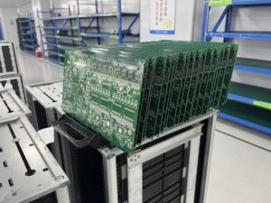
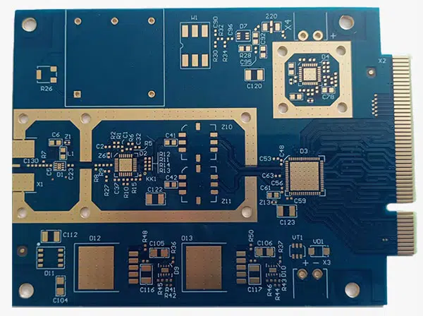
مورد لوحات الدوائر المطبوعة عالية الكثافة
South-Electronic
اختر شركة South-Electronic لأعلى مستويات الجودة والموثوقية وأفضل قيمة لاحتياجاتك في مجال لوحات الدوائر المطبوعة. اختبر الفارق مع خدمات HDI الشاملة لدينا – من التصميم إلى الإنتاج، نحن نضمن الدقة، والمتانة، والامتثال لأصعب معايير الصناعة.
شريكك الموثوق للوحات الدوائر المطبوعة عالية الجودة HDI
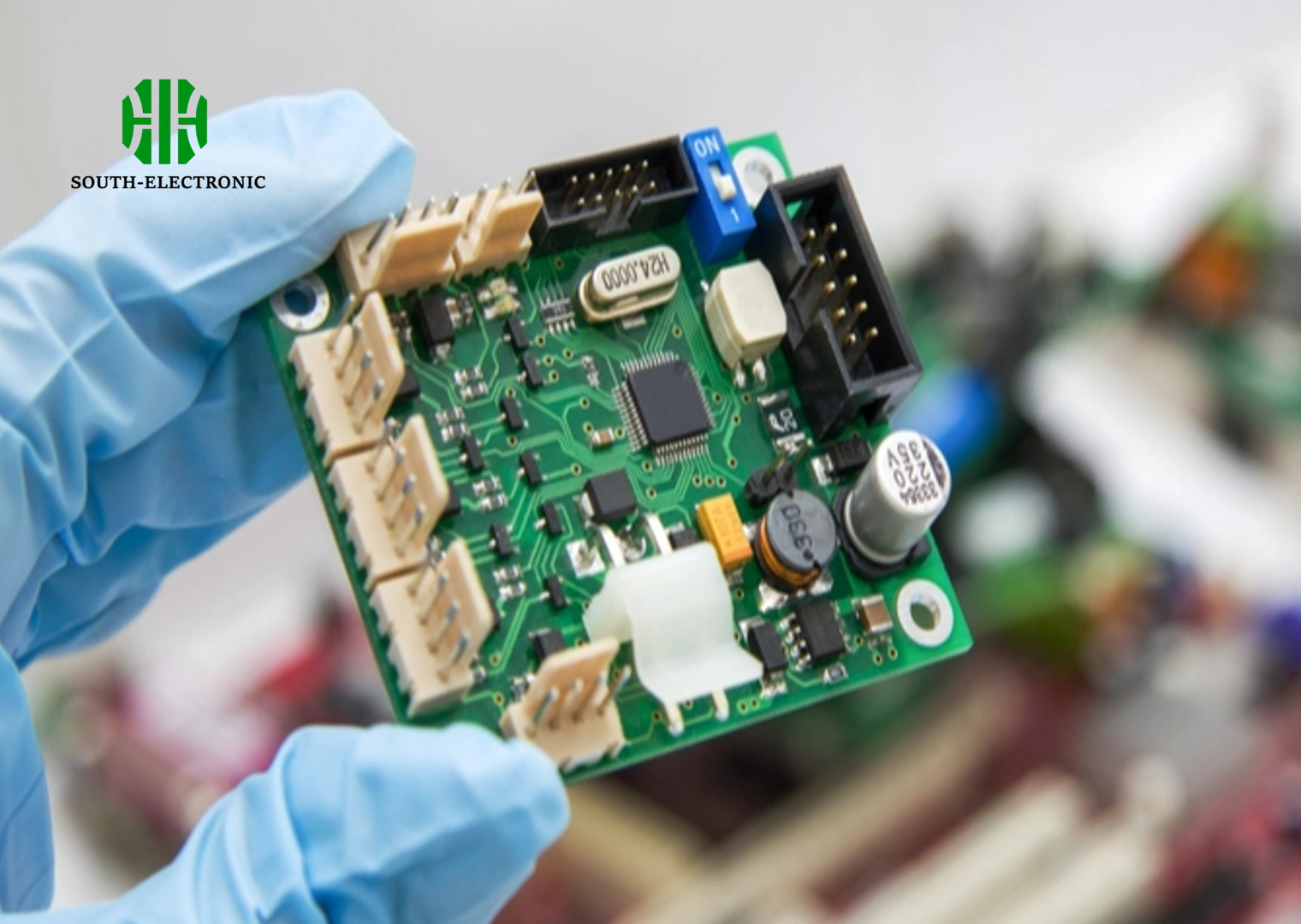
مرحبًا بك في شركة South-Electronic، مصدر لوحات الدوائر المطبوعة عالية الكثافة عالية الجودة، والمعروفة بتقنية الوصلات ذات الكثافة العالية وقدرات التصغير.
ثق في South-Electronic للحصول على جودة واتساق عاليين في مشاريعك التقنية. لوحات الدوائر المطبوعة HDI لدينا تعزز أداء أجهزتك من خلال الاتصال الاستثنائي وتقليل المساحة المطلوبة. تعاون معنا لتحقيق الابتكار والنجاح في مجالك.
النوع الأول من لوحات الدوائر المطبوعة عالية الكثافة
هذا النوع يحتوي على مايكروفياس فائقة الدقة بأقطار أقل من 75 ميكرون وعرض/عزل الموصلات أقل من 50 ميكرون. إنه مثالي للأجهزة الإلكترونية من الجيل التالي، مثل المعدات الطبية المتقدمة والاتصالات عالية التردد.

النوع الثاني من لوحات الدوائر المطبوعة عالية الكثافة
هذا النوع يعتمد على النوع الأول عن طريق إضافة الفتحات العمياء والمدفونة لتحسين التوجيه. إنه مناسب للأجهزة الإلكترونية المتقدمة التي تتطلب اتصالات متعددة الطبقات المعقدة وكثافة أعلى.
النوع الثالث من لوحات الدوائر المطبوعة عالية الكثافة
هذا النوع يحتوي على طبقتين على الأقل من المايكروفياس على جانب واحد أو كلا الجانبين من النواة، باستخدام الفتحات العمياء والمدفونة. إنه ممتاز للتطبيقات عالية الأداء مثل الهواتف الذكية والحوسبة المتقدمة لأنه يوفر توجيهًا فائقًا.
لوحات الدوائر المطبوعة فائقة الدقة عالية الكثافة
هذا النوع يحتوي على مايكروفياس فائقة الدقة بأقطار أقل من 75 ميكرون وعرض/عزل الموصلات أقل من 50 ميكرون. إنه مثالي للأجهزة الإلكترونية من الجيل التالي، مثل المعدات الطبية المتقدمة والاتصالات عالية التردد.
لماذا تختار South-Electronic؟
اختر South-Electronic لخبرتنا في إنتاج لوحات الدوائر المطبوعة عالية الكثافة المخصصة وعالية الجودة لمجموعة متنوعة من التطبيقات. يتمتع فريقنا بخبرة واسعة، مما يضمن جودة فائقة بأسعار تنافسية وخدمة استثنائية من البداية إلى النهاية.
-
مرونة في الطلب
يمكنك طلب قطعة واحدة فقط لتلبية احتياجاتك المحددة من لوحات HDI.
استمتع بالمرونة في اختبار التصاميم الجديدة أو تلبية متطلبات الدفعات الصغيرة دون أي متاعب. -
فريق ذو خبرة
تستفيد من خبرتنا التي تمتد لعقد في هذا المجال.
نحن نفهم التحديات التي تواجهك ونوفر حلولًا احترافية ودعمًا موثوقًا في كل خطوة. -
خدمة شاملة
تحصل على رضا تام مع مجموعة واسعة من المعدات لدينا.
تضمن خدمتنا الشاملة حصولك على كل ما تحتاجه لتجربة سلسة. -
توصيل سريع
تستفيد من أوقات الإنتاج السريعة والفعالة لدينا.
نحن نعطي الأولوية للتسليم في الوقت المناسب للوفاء بالمواعيد النهائية والحفاظ على مشاريعك على المسار الصحيح. -
ضمان الرضا
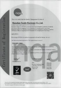
نضمن لك الجودة والتواصل الواضح مع شهادة ISO9001 لدينا.
رضاك هو أولويتنا، ونحن ملتزمون بتجاوز توقعاتك مع كل طلب.
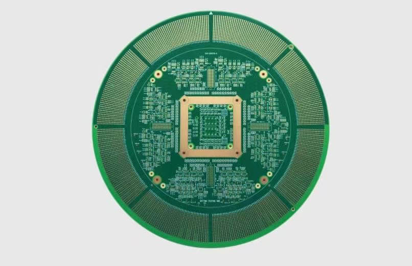
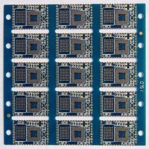
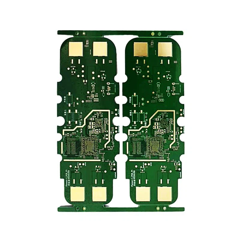
مشاريع ذات صلة قمنا بها
آراء العملاء
الأسئلة الشائعة
الأسئلة الأكثر شيوعًا
أرسل لنا رسالة
كلما كانت التفاصيل أكثر دقة، كلما تمكنا من المضي قدمًا إلى الخطوة التالية أسرع.


الدليل الكامل للوحات الدوائر المطبوعة عالية الكثافة (HDI)
محتويات
الفصل 1
مقدمة إلى لوحات الدوائر المطبوعة عالية الكثافة
ما هي لوحة الدوائر المطبوعة HDI؟
لوحات الدوائر المطبوعة عالية الكثافة (HDI) هي لوحات دوائر متقدمة مصممة لاستيعاب كثافة أسلاك أعلى لكل وحدة مساحة، باستخدام آثار رقيقة ومايكروفياس. يسمح هذا بتوجيه أكثر تعقيدًا ودمج المكونات في تصميم مضغوط، مما يجعل تقنية HDI مثالية للتطبيقات عالية الأداء.
لماذا هي مهمة وأين تُستخدم؟
تعتبر لوحات الدوائر المطبوعة عالية الكثافة (HDI) ضرورية في الإلكترونيات الحديثة، حيث تعمل على تشغيل الأجهزة التي تتطلب معالجة أسرع، وكفاءة أعلى، وأحجام أصغر. تُستخدم على نطاق واسع في الهواتف الذكية، وأجهزة الكمبيوتر المحمولة، والأجهزة الطبية، وأنظمة السيارات، ومعدات الاتصالات المتقدمة. ومع استمرار نمو متطلبات التكنولوجيا، تمكن لوحات HDI المصنعين من تلبية احتياجات حلول إلكترونية أكثر إحكامًا وكفاءة وموثوقية.
الفصل 2
أنواع تكوينات لوحات الدوائر المطبوعة عالية الكثافة
أنواع مختلفة من تكوينات لوحات HDI
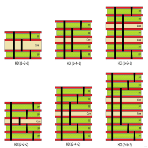
هناك طرق مختلفة لتكوين لوحات HDI، وذلك حسب مدى تعقيدها والوظائف التي تحتاجها. التكوين الأساسي هو تصميم HDI من خطوة واحدة، والذي يحتوي على طبقة واحدة من المايكروفياس التي توفر اتصالاً فعالاً للتطبيقات الأقل تطلبًا، مثل الإلكترونيات الاستهلاكية الصغيرة. يعتمد تصميم HDI المكون من خطوتين على هذا التصميم بإضافة طبقة أخرى من المايكروفياس أو الفتحات المتداخلة، مما يزيد من كثافة اللوحة ويسمح بتوجيه إشارات أكثر تعقيدًا. أما التكوين الأكثر تقدماً فهو تصميم HDI متعدد الخطوات، الذي يستخدم فتحات مكدسة أو متداخلة عبر طبقات متعددة لتحقيق أقصى كثافة والتعامل مع تصميمات الدوائر المعقدة للغاية. هذه التكوينات مهمة للتطبيقات المتقدمة مثل الحوسبة عالية السرعة، والاتصالات، والمعدات العسكرية، حيث الأداء، والموثوقية، وتحسين المساحة هي أمور حاسمة.
توضيح المايكروفياس، الفتحات العمياء، والفتحات المدفونة
تستخدم تقنية HDI أنواعاً متقدمة من الفتحات لزيادة خيارات التوجيه والاتصال بين طبقات PCB بشكل كبير. المايكروفياس هي فتحات صغيرة جداً محفورة بالليزر، ويبلغ قطرها عادةً أقل من 0.15 مم. إنها تربط الطبقات المجاورة وتسمح بوضع مكونات كثيف وسلامة إشارات عالية. الفتحات العمياء تربط الطبقة الخارجية للوحة بطبقة أو أكثر من الطبقات الداخلية دون المرور عبر اللوحة بأكملها، مما يوفر مساحة على سطح PCB مع الحفاظ على كفاءة التوجيه. أما الفتحات المدفونة فتربط فقط الطبقات الداخلية وتكون مخفية تمامًا عن الخارج، مما يسمح للمصممين بإنشاء تصاميم أكثر تعقيدًا دون التضحية بالمساحة السطحية لإضافة مكونات أخرى.
فوائد التكوينات المختلفة للوحة HDI
يعتمد اختيار التكوين المناسب لـ HDI على التطبيق المحدد ومتطلبات الأداء. تصميم HDI من خطوة واحدة اقتصادي ومثالي للمنتجات التي تتطلب أداءً معتدلًا، مثل الأجهزة القابلة للارتداء أو الإلكترونيات الاستهلاكية الأساسية. تتيح تكوينات HDI ذات الخطوتين والمتعددة كثافة مكونات أعلى ودوائر أكثر تعقيدًا، وهو أمر ضروري للتطبيقات المتقدمة مثل الهواتف الذكية، والأجهزة اللوحية، والأجهزة الطبية، وإلكترونيات السيارات. بالإضافة إلى ذلك، فإن استخدام المايكروفياس، والفتحات العمياء، والفتحات المدفونة يحسن من مساحة اللوحة، ويقلل من التداخلات، ويحسن من إدارة الحرارة، ويعزز الأداء العام، خاصة في الأجهزة التي تتطلب نقل بيانات عالية السرعة وتصغير الحجم، مثل معدات الاتصالات، وأنظمة الطيران، وأجهزة الحوسبة عالية الأداء. باستخدام هذه التكوينات المختلفة وتقنيات الفتحات، توفر لوحات HDI مرونة تصميم لا مثيل لها، وتحسينًا في الأداء، وفوائد توفير المساحة، والتي تعتبر ضرورية للإلكترونيات الحديثة.
الفصل 3

عملية تصنيع لوحات الدوائر المطبوعة عالية الكثافة
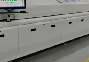
تعتبر عملية تصنيع لوحات HDI معقدة، حيث تتطلب العديد من الخطوات والتقنيات المتقدمة. الهدف هو إنشاء تصميم عالي الكثافة متعدد الطبقات قادر على التعامل مع متطلبات الإلكترونيات الحديثة من حيث التصغير والسرعة والأداء. إليك تفصيل مفصل للخطوات والتقنيات الرئيسية المستخدمة في تصنيع لوحات HDI.
عملية التصنيع خطوة بخطوة
تبدأ عملية تصنيع لوحات HDI بتكوين طبقة أساسية، والتي تُعد الأساس للطبقات الأخرى. تتم إضافة طبقات إضافية عن طريق الترقيق والنقش لتشكيل مسارات الدائرة المعقدة. ثم تُستخدم تقنيات متقدمة للفتحات، مثل المايكروفياس، الفتحات العمياء، والفتحات المدفونة، لتوصيل الطبقات. بعد إعداد الفتحات، تخضع اللوحة للحفر، وترسيب النحاس، وإنهاء السطح. ثم يتم فحصها واختبارها للتأكد من توافقها مع المواصفات ومعايير الجودة قبل إرسالها إلى العميل.
- تكوين الطبقة الأساسية: تبدأ العملية بتكوين طبقات اللوحة الأساسية، حيث يتم ترقيق طبقات النحاس والعازل معًا.
- الحفر بالليزر: يتم إنشاء المايكروفياس باستخدام حفر الليزر عالي الدقة. هذه خطوة حاسمة في تصنيع لوحات HDI لأنها تسمح بإنشاء فتحات صغيرة جدًا (عادةً أقل من 150 ميكرون) تربط الطبقات الداخلية والخارجية.
- ترسيب النحاس والطلاء: بعد حفر الفتحات، تخضع اللوحة لترسيب النحاس، حيث يتم وضع طبقة رقيقة من النحاس على جدران الفتحات. تضمن هذه الخطوة توصيلًا كهربائيًا بين الطبقات. ثم يتم طلاء السطح بأكمله بالنحاس عبر الطلاء الكهربائي لتشكيل الآثار الموصلة.
- الترقيق: يتم تكديس طبقات PCB المتعددة وربطها معًا بواسطة الترقيق، حيث يتم تطبيق الحرارة والضغط لربط طبقات النحاس والمواد العازلة المختلفة، مما يشكل هيكلًا متعدد الطبقات ضروريًا للتصاميم عالية الكثافة.
- النقش وتشكيل الدوائر: يتم نقش طبقات النحاس بشكل انتقائي لتشكيل النمط المطلوب للدائرة. هذه خطوة حاسمة في إنشاء مسارات الإشارة على اللوحة.
- إنهاء السطح وتطبيق قناع اللحام: يتم وضع قناع اللحام لحماية الآثار النحاسية ومنع حدوث دوائر قصيرة عند لحام المكونات. ثم يتم وضع تشطيب سطحي، مثل ENIG (نيكل غير كهربائي-ذهب غامر) أو HASL (تسوية اللحام بالهواء الساخن)، لتحسين قابلية اللحام ومنع الأكسدة.
- الفحص والاختبار: يتم اختبار المنتج النهائي بدقة، بما في ذلك الفحص البصري الآلي (AOI)، والاختبار الكهربائي، وأحيانًا الفحص بالأشعة السينية، للتأكد من أن جميع التوصيلات تعمل وأن PCB تلبي المواصفات التصميمية.
التقنيات المستخدمة
يعتمد تصنيع لوحات HDI على العديد من التقنيات المتقدمة التي تتيح تحقيق الدقة العالية:
- الحفر بالليزر: يُستخدم لإنشاء المايكروفياس، وهي مفتاح تصميم HDI عالي الكثافة. يتيح الحفر بالليزر إنشاء فتحات صغيرة جدًا لا يمكن للحفر الميكانيكي إنشاؤها.
- الترقيق: يربط هذا العملية الطبقات المتعددة من النحاس والمواد العازلة معًا، مما يخلق هياكل PCB متعددة الطبقات HDI. يضمن الترقيق أن تكون اللوحة قوية ومستقرة ميكانيكيًا.
- الطلاء: يُستخدم الطلاء الكهربائي لوضع النحاس على الفتحات والمسارات، مما يضمن وجود اتصال كهربائي جيد بين الطبقات. كما تُستخدم تشطيبات سطحية خاصة مثل ENIG أو OSP (مادة حافظة للتلحيم العضوي) لجعل اللوحة أكثر متانة وأسهل في اللحام.
المواد الأساسية المستخدمة في تصنيع لوحات HDI
يعتبر اختيار المواد مهمًا لتصنيع لوحات HDI من حيث الأداء والموثوقية:
- رقائق النحاس: يُستخدم النحاس لإنشاء المسارات الموصلة والفتحات في اللوحة. يتميز بتوصيله الكهربائي العالي، مما يجعله جيدًا لضمان كفاءة الإشارات.
- المواد العازلة: تُستخدم مواد مثل FR-4 (راتنج الإيبوكسي المقوى بالزجاج) كطبقات عازلة بين طبقات النحاس. وللتصاميم الأكثر تقدمًا، يمكن استخدام مواد ذات ثبات حراري أعلى، مثل البوليميد.
- البريبرغ والرقائق: تعتبر هذه المواد مهمة لربط الطبقات معًا. يُوضع البريبرغ (نسيج زجاجي مغطى بالراتنج) بين طبقات النحاس أثناء الترقيق لضمان قوة اللوحة الكهربائية والعزل.
- قناع اللحام: يُوضع طبقة حماية فوق الآثار النحاسية لمنع الأكسدة والدوائر القصيرة أثناء التجميع.
- تشطيبات السطح: تُستخدم تشطيبات شائعة مثل ENIG، HASL، أو OSP لحماية النحاس المكشوف وجعل لحام المكونات أسهل.
باختصار، يعتبر تصنيع لوحات HDI عملية معقدة تتطلب التحكم الدقيق في كل خطوة واستخدام مواد وتقنيات متقدمة. يجمع التصنيع بين الحفر بالليزر، والترقيق متعدد الطبقات، والمواد عالية الأداء لصنع لوحات صغيرة وعالية الكثافة تعتبر أساسية للأجهزة الإلكترونية الحديثة.
الفصل 4
مزايا لوحات الدوائر المطبوعة عالية الكثافة
توفر لوحات HDI العديد من المزايا مقارنة بتصميمات PCB التقليدية، مما يجعلها أساسية في الإلكترونيات الحديثة حيث تكون المساحة والأداء والكفاءة أموراً حاسمة. فيما يلي الفوائد الرئيسية التي تجعل تقنية HDI الخيار المفضل للأجهزة عالية الأداء والمدمجة والموثوقة:
زيادة الكثافة وتكامل المكونات
أحد المزايا الأساسية للوحات HDI هو قدرتها على دعم كثافة مكونات أعلى بكثير من لوحات PCB القياسية. باستخدام المايكروفياس، والفتحات العمياء، والفتحات المدفونة، يمكن للوحات HDI دمج المزيد من المكونات في مساحة أصغر. يسمح هذا بتوجيه معقد، خاصة في التصميمات متعددة الطبقات، مما يمكن المهندسين من إنشاء دوائر معقدة دون التضحية بالمساحة أو الوظيفة. تُعد هذه الكثافة المتزايدة ضرورية للتطبيقات المتقدمة مثل الهواتف الذكية، والأجهزة القابلة للارتداء، وإلكترونيات السيارات، حيث تكون مساحة اللوحة المتاحة محدودة، لكن الطلب على الوظائف مرتفع.
تحسين الأداء الكهربائي وسلامة الإشارة
تم تصميم لوحات HDI للتعامل مع إشارات عالية السرعة مع تقليل فقد الإشارة والتداخل إلى الحد الأدنى. يقلل استخدام المسارات القصيرة والمايكروفياس من طول مسار الإشارة، مما يقلل من التداخل الكهرومغناطيسي (EMI) والتداخل المتبادل. يؤدي ذلك إلى تحسين سلامة الإشارة، وهو أمر مهم للتطبيقات عالية التردد مثل اتصالات 5G، والأجهزة المتصلة بالإنترنت (IoT)، وأنظمة الحوسبة. بالإضافة إلى ذلك، فإن القدرة على وضع المكونات بالقرب من بعضها يقلل من مسارات الإشارات، مما يقلل من التأخير في الإشارة ويحسن الأداء العام، خاصة في التطبيقات التي تتطلب بيانات مكثفة حيث تكون السرعة والدقة أمرين حاسمين.
شكل أصغر وتصميمات أكثر إحكامًا
يعتبر تصغير الإلكترونيات قوة دافعة وراء التبني الواسع لتقنية HDI. تسمح لوحات HDI للمصنعين بإنشاء أجهزة أصغر وأرق وأخف وزناً دون التضحية بالوظائف أو الأداء. من خلال تحقيق أقصى استفادة من مساحة اللوحة المتاحة باستخدام التوجيه عالي الكثافة والهياكل متعددة الطبقات، تساعد لوحات HDI في تقليل الحجم الإجمالي للأجهزة. هذا مهم بشكل خاص في الأجهزة الإلكترونية الاستهلاكية المحمولة، مثل الهواتف الذكية والأجهزة اللوحية والأجهزة القابلة للارتداء، حيث تُعتبر الأشكال المدمجة ليست مرغوبة فحسب، بل ضرورية للاستخدام العملي.
زيادة الموثوقية والمتانة
يساهم البناء المتقدم للوحات HDI في زيادة الموثوقية والمتانة مقارنةً باللوحات التقليدية. تسمح الفتحات الأصغر وزيادة عدد الوصلات بتحسين إدارة الحرارة، حيث يتم توزيع الحرارة بشكل أكثر تساويًا عبر اللوحة. هذا يقلل من خطر النقاط الساخنة وفشل المكونات بسبب الحرارة المفرطة. علاوة على ذلك، فإن المواد المستخدمة في لوحات HDI، مثل الرقائق عالية الأداء والنحاس، توفر مقاومة أفضل للإجهاد الميكانيكي، مما يضمن سلامة اللوحة حتى في ظل الظروف البيئية القاسية. هذا يجعل لوحات HDI مثالية للصناعات مثل السيارات، والطيران، والعسكرية، حيث تكون المتانة والموثوقية أموراً أساسية.
نقل أسرع للإشارة وتحسين الأداء
بالإضافة إلى سلامة الإشارة الأفضل، توفر لوحات HDI نقل أسرع للإشارة بفضل تصميمها المتقدم. تساهم مسارات الإشارة القصيرة، وتأخير الإشارة المنخفض، والتوجيه الأمثل في سرعات نقل البيانات الأسرع، وهو أمر مهم في التطبيقات التي تتطلب طاقة معالجة عالية ونقل بيانات سريع. تُستخدم لوحات HDI على نطاق واسع في قطاعات مثل الاتصالات، والحوسبة، والأتمتة الصناعية، حيث تكون معالجة البيانات عالية السرعة والتواصل أمورًا حاسمة لأداء النظام.
مرونة في التصميم والتخصيص
تسمح مرونة تصميمات لوحات HDI للمهندسين بإنشاء لوحات مخصصة تناسب الاحتياجات التطبيقية المحددة. مع تكوينات الفتحات المتعددة وإمكانية تكديس الطبقات بطرق مختلفة، توفر لوحات HDI حرية تصميم أكبر مقارنةً بلوحات PCB التقليدية. هذا يجعلها مثالية لإنشاء حلول مخصصة للصناعات المتخصصة مثل الأجهزة الطبية، حيث تكون التصميمات الفريدة مطلوبة غالبًا لتلبية معايير الحجم والأداء الصارمة. تعزز القدرة على دمج تصميمات PCB المرنة-الصلبة من هذه المرونة، مما يسمح بتخطيطات ثلاثية الأبعاد معقدة يمكن أن تتناسب مع أجهزة مدمجة أو غير منتظمة الشكل.
كفاءة التكلفة في الإنتاج بكميات كبيرة
على الرغم من أن التكلفة الأولية لإنتاج لوحات HDI قد تكون أعلى بسبب تقنيات التصنيع المتقدمة، إلا أن هذه التكاليف تتعوض في عمليات الإنتاج بكميات كبيرة. حيث يسمح تكامل المزيد من الوظائف في مساحة أصغر بتقليل الحاجة إلى لوحات متعددة ومكونات ووصلات، مما يقلل من التكلفة الإجمالية للمنتج النهائي. بالإضافة إلى ذلك، يؤدي تحسين موثوقية وأداء لوحات HDI إلى تقليل عدد الأعطال، مما يقلل التكاليف المرتبطة بالإصلاحات والعائدات وتوقف العمل، مما يجعل تقنية HDI حلاً فعالًا من حيث التكلفة على المدى الطويل للمصنعين بكميات كبيرة.
باختصار، توفر لوحات HDI مجموعة من المزايا التي تجعلها الحل الأمثل للمصنعين الذين يهدفون إلى إنشاء منتجات إلكترونية عالية الأداء، مدمجة، وموثوقة. إن قدرتها على دعم كثافة مكونات أكبر، وتحسين سلامة الإشارة، وتوفير سرعات أعلى، وتعزيز مرونة التصميم جعلتها لا غنى عنها في قطاعات مثل الإلكترونيات الاستهلاكية، والاتصالات، والسيارات، والطيران، والأجهزة الطبية. ومع استمرار تطور التكنولوجيا، ستزداد الحاجة إلى لوحات HDI، مما يدفع الابتكار ويمكّن من تطوير أنظمة إلكترونية أكثر تقدمًا وصغرًا.

الفصل 5
التطبيقات الشائعة للوحات الدوائر المطبوعة عالية الكثافة
أصبحت لوحات HDI ضرورية في مجموعة واسعة من الصناعات بفضل قدرتها على دعم التصميمات عالية الكثافة، والأداء الكهربائي المحسّن، والأحجام الصغيرة. تجعل ميزاتها المتقدمة وتعدد استخداماتها مثالية للعديد من التطبيقات عبر مختلف القطاعات التقنية. فيما يلي بعض التطبيقات الأكثر شيوعًا للوحات HDI:
الإلكترونيات الاستهلاكية
يعتمد سوق الإلكترونيات الاستهلاكية، خاصةً الأجهزة مثل الهواتف الذكية، الأجهزة اللوحية، أجهزة الكمبيوتر المحمولة، والأجهزة القابلة للارتداء، بشكل كبير على لوحات HDI. مع تزايد الطلب على الأجهزة الأصغر والأقوى وذات الميزات المتعددة، تتيح تقنية HDI للمصنعين زيادة الوظائف إلى أقصى حد مع تقليل الحجم.
- الهواتف الذكية: تمكّن لوحات HDI من دمج ميزات متقدمة مثل الكاميرات عالية الدقة، المعالجات السريعة، الاتصال بشبكات 5G، وعمر بطارية محسن في مساحة مضغوطة للغاية.
- الأجهزة اللوحية وأجهزة الكمبيوتر المحمولة: تستفيد هذه الأجهزة من لوحات HDI من خلال توفير معالجة بيانات أسرع، إدارة طاقة أفضل، واستخدام أكثر كفاءة للمساحة، مما يؤدي إلى تصميمات أنحف ومنتجات أخف وزنًا.
- الأجهزة القابلة للارتداء: تستخدم أجهزة مثل الساعات الذكية وأجهزة تتبع اللياقة البدنية لوحات HDI لدمج مستشعرات متعددة، معالجات، ووحدات اتصال لاسلكي في حزمة صغيرة وخفيفة الوزن، مما يجعلها مريحة للارتداء مع توفير وظائف قوية.
الأجهزة الطبية ومعدات الرعاية الصحية
تلعب لوحات HDI دورًا حيويًا في تطوير الأجهزة الطبية، حيث يكون الدقة والموثوقية والحجم الصغير أمورًا حاسمة. مع اعتماد صناعة الرعاية الصحية لتقنيات أكثر تقدمًا مثل الأجهزة التشخيصية المحمولة، المعدات الطبية القابلة للزرع، وأنظمة المراقبة، زاد استخدام لوحات HDI بشكل كبير.
- الأجهزة القابلة للزرع: تُستخدم لوحات HDI في أجهزة مثل منظمات ضربات القلب، ومحفزات الأعصاب، وأجهزة السمع، حيث تكون الحجم الصغير والموثوقية ضرورية للاستخدام الآمن على المدى الطويل داخل جسم الإنسان.
- معدات التشخيص: تستفيد الأجهزة مثل أجهزة الموجات فوق الصوتية، ماسحات MRI، والأدوات التشخيصية المحمولة من قوة المعالجة العالية وكفاءة نقل البيانات التي توفرها لوحات HDI، مما يضمن نتائج دقيقة وفي الوقت المناسب.
- أجهزة مراقبة الصحة القابلة للارتداء: تتطلب أجهزة تتبع اللياقة والأجهزة الطبية القابلة للارتداء التي تراقب معدل ضربات القلب، وضغط الدم، وغيرها من العلامات الحيوية، لوحات HDI المدمجة والخفيفة الوزن لتقديم أداء موثوق بينما تكون مريحة للمريض.
صناعات السيارات والطيران
في قطاعي السيارات والطيران، تعد لوحات HDI ضرورية لإنشاء أنظمة عالية الأداء وموثوقة قادرة على تحمل الظروف البيئية القاسية مع تقديم وظائف متقدمة.
- إلكترونيات السيارات: تُستخدم لوحات HDI في أنظمة مساعدة السائق المتقدمة (ADAS)، وأنظمة الترفيه والمعلومات، والتحكم في الملاحة، ووحدات إدارة الطاقة. إن حجمها الصغير وموثوقيتها العالية وقدرتها على نقل البيانات بسرعة عالية تجعلها ضرورية للسيارات الحديثة، خاصةً السيارات الكهربائية والمستقلة.
- أنظمة الطيران: تُستخدم لوحات HDI في الأنظمة الإلكترونية للطائرات، ومعدات الاتصالات الفضائية، وأنظمة التحكم في الملاحة. يجب أن تتحمل هذه اللوحات درجات الحرارة القصوى، وتغيرات الضغط، والاهتزازات، وتضمن تقنية HDI موثوقية عالية وأداءً في هذه الظروف القاسية. بالإضافة إلى ذلك، يساهم وزن لوحات HDI الخفيف في تقليل الوزن الإجمالي للطائرات والمركبات الفضائية، مما يعد عاملًا حاسمًا في تصميم الطيران.
معدات الاتصالات والشبكات
يعد قطاع الاتصالات من المجالات التي تؤثر فيها لوحات HDI بشكل كبير. مع ظهور تقنية 5G، أصبحت الحاجة إلى نقل بيانات عالي السرعة وترددات عالية أمورًا ضرورية، وتوفر لوحات HDI الأداء والتصغير اللازمين لتلبية هذه المتطلبات.
- محطات قاعدة 5G: تُستخدم لوحات HDI في البنية التحتية الأساسية لشبكات 5G، مما يتيح معدلات نقل بيانات أسرع، وتأخير أقل، وعرض نطاق ترددي أعلى. تساعد في تحقيق تصميمات الخلايا الصغيرة المطلوبة لنشر تقنية 5G.
- أجهزة التوجيه والمفاتيح الشبكية: في أجهزة الشبكات، تتيح لوحات HDI توجيه إشارات عالية السرعة بكفاءة مع تقليل التداخل وفقدان الإشارة. يضمن هذا أن تعمل أجهزة التوجيه، والمفاتيح، ومراكز البيانات بأداء مثالي، مما يسهل التواصل السلس ونقل البيانات عبر شبكات واسعة النطاق.
- أنظمة اتصالات الألياف البصرية: تُعد لوحات HDI ضرورية في المحولات البصرية ومعالجات الإشارة، التي تعد مكونات حاسمة في أنظمة الاتصالات بالألياف البصرية. تضمن تصميماتها عالية الكثافة معالجة بيانات فعالة وسرعات نقل عالية.
الأتمتة الصناعية والروبوتات
يستفيد مجال الأتمتة الصناعية والروبوتات المتنامي أيضًا من لوحات HDI. تعتمد أنظمة الأتمتة على معالجة دقيقة وسريعة للبيانات للتحكم في الآلات والمستشعرات والمحركات في الوقت الفعلي.
- الروبوتات: تُستخدم لوحات HDI في الروبوتات لأنظمة الملاحة، ووحدات التحكم في المحركات، ووحدات المعالجة، حيث تكون المساحة محدودة، والأداء حاسم. تتطلب هذه الأنظمة غالبًا نقل بيانات عالي السرعة، واستهلاك طاقة منخفض، وموثوقية عالية، وكلها يمكن أن توفرها لوحات HDI.
- وحدات التحكم في الأتمتة: تُستخدم لوحات HDI في وحدات التحكم المنطقية القابلة للبرمجة (PLCs) وواجهات الإنسان والآلة (HMIs) التي تتحكم في الآلات الصناعية، مما يضمن عملها بكفاءة ودقة في بيئات التصنيع المعقدة.
6. الأنظمة العسكرية والدفاعية
في القطاعين العسكري والدفاعي، تُعد لوحات HDI لا غنى عنها بفضل موثوقيتها العالية، وحجمها الصغير، وقدرتها على تحمل الظروف القاسية. تتطلب أنظمة الدفاع غالبًا إلكترونيات قوية للتطبيقات مثل الاتصالات، والمراقبة، والرادار، وأنظمة الأسلحة.
- أنظمة الرادار والاتصالات: تضمن لوحات HDI معالجة البيانات بسرعة والاتصال الموثوق في الأنظمة العسكرية الحيوية، حيث لا تكون هناك فرصة للتوقف أو الفشل.
- أنظمة التحكم في الأسلحة: تُستخدم لوحات HDI في أنظمة التوجيه للصواريخ والطائرات بدون طيار، حيث يكون الحجم الصغير والدقة العالية أمرين أساسيين.
باختصار، تُستخدم لوحات HDI في مجموعة واسعة من الصناعات والتطبيقات، بدءًا من الإلكترونيات الاستهلاكية والرعاية الصحية وصولاً إلى السيارات، والطيران، والاتصالات، والدفاع. قدرتها على توفير تصميمات عالية الكثافة والأداء العالي والأحجام الصغيرة تجعلها أساسية للتقنيات المتقدمة اليوم والأنظمة الإلكترونية المعقدة. ومع تزايد الطلب على الإلكترونيات الأصغر والأسرع والأكثر كفاءة، سيستمر استخدام لوحات HDI في التوسع عبر هذه الصناعات.
الفصل 6
تصميم لوحات الدوائر المطبوعة عالية الكثافة
يعد تصميم لوحات HDI مهمة معقدة تتطلب مراعاة دقيقة لمختلف العوامل لزيادة الأداء، وضمان الموثوقية، وتلبية المتطلبات المحددة للتطبيقات الإلكترونية عالية الكثافة وعالية السرعة. في هذه المقالة، سنوضح بعض الإرشادات التي تساعدك على تصميم لوحات HDI تلبي هذه المتطلبات.
أفضل الممارسات لتصميم لوحات HDI
يعد تصميم لوحات HDI أكثر تعقيدًا من تصميم لوحات PCB التقليدية نظرًا للكثافة العالية وتقنيات التصنيع المتقدمة المستخدمة. يمكن أن يساعد اتباع أفضل الممارسات في ضمان تصميم مثالي:
- تحديد أهداف تصميم واضحة: ابدأ بتحديد متطلبات أداء المنتج بوضوح، مثل سرعة الإشارة، كثافة المكونات، والقيود الميكانيكية. سيساعدك هذا في اختيار تكوين HDI المناسب، بما في ذلك عدد الطبقات وهياكل الفتحات.
- التعاون المبكر مع المصنعين: يرتبط تصميم لوحات HDI بشكل وثيق بقدرات التصنيع. يضمن التعاون مع الشركة المصنعة مبكرًا في عملية التصميم إمكانية إنتاج التصميم بتكلفة فعالة وضمن الحدود التقنية للشركة المصنعة، مما يتيح تجنب التكرارات المكلفة.
- استخدام برامج تصميم متقدمة: تتطلب لوحات HDI الحديثة أدوات تصميم متقدمة تدعم التصميمات متعددة الطبقات وعالية الكثافة والمايكروفياس والعرض الدقيق للآثار. يضمن استخدام برامج متطورة مثل Altium Designer أو Cadence Allegro دقة أكبر والامتثال لمعايير التصنيع.
- تطبيق تصميم قابل للتصنيع (DFM): يجب مراعاة قابلية التصنيع طوال عملية التصميم عن طريق تجنب الهياكل المعقدة التي قد تؤدي إلى زيادة التكاليف أو انخفاض معدلات الإنتاج. تشمل إرشادات DFM الحفاظ على أحجام الفتحات ضمن نطاقات التصنيع، وتقليل عدد الثقوب، وضمان تباعد مناسب للنحاس.
اعتبارات التخطيط: عرض الأثر، وضع الفتحات، وتصميم التكديس
يعد تخطيط لوحة HDI أمرًا بالغ الأهمية لتحقيق الأداء العالي، خاصةً من حيث سلامة الإشارة، وإدارة الحرارة، ووضع المكونات. تتطلب عدة عناصر في التخطيط تخطيطًا دقيقًا:
- عرض الأثر والمسافات: نظرًا لأن لوحات HDI تتعامل غالبًا مع إشارات عالية السرعة، يجب حساب عرض الأثر والمسافات بعناية لتقليل فقدان الإشارة وتجنب التداخل. من الضروري الحفاظ على التحكم في المعاوقة بناءً على سرعة الإشارة ونوع خط النقل (مثل microstrip أو stripline). في التطبيقات عالية التردد، قد يصل عرض الأثر إلى 3-5 مل، ويجب تحسين التباعد لتقليل الضوضاء.
- وضع الفتحات وأنواعها: يعد وضع الفتحات بشكل صحيح أمرًا أساسيًا للحفاظ على سلامة الإشارات التي تنتقل بين الطبقات. تُستخدم المايكروفياس في لوحات HDI نظرًا لصغر حجمها، مما يسمح بوضع مكونات كثيفة. من المهم وضع الفتحات بالقرب من المكونات لتقصير مسارات الإشارات، مما يحسن سرعة النقل ويقلل من تدهور الإشارة. يجب استخدام الفتحات العمياء والمدفونة بشكل استراتيجي للحفاظ على تماسك اللوحة وتجنب الطبقات الزائدة. بالإضافة إلى ذلك، يمكن أن توفر الفتحات المتراكبة توصيلًا معززًا بين الطبقات ولكن يجب استخدامها باعتدال للتحكم في التكاليف وضمان الثبات الميكانيكي.
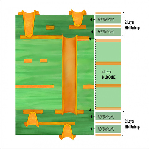
- تصميم التكديس: يشير تصميم تكديس لوحة HDI إلى ترتيب طبقاتها، بما في ذلك طبقات الإشارة، والطاقة، والأرضي. يساعد التكديس الأمثل في تحقيق التحكم في المعاوقة، ويحسن سلامة الإشارة، ويقلل من التداخل الكهرومغناطيسي (EMI). عادةً ما يتم استخدام طبقات إشارة وأرضي متناوبة لتوفير الحماية الكافية والحفاظ على المعاوقة المتسقة عبر الآثار عالية السرعة. يفضل أيضًا التكديس المتماثل لتجنب التشوه أثناء عملية التصنيع. في التصميمات المعقدة، تُستخدم طبقات إضافية مع الفتحات العمياء والمدفونة لتقليل عدد الطبقات اللازمة للتوجيه، مما يعزز جودة الإشارة ويقلل من سمك اللوحة.
كيفية تقليل تداخل الإشارة وتحسين إدارة الحرارة
تُستخدم لوحات HDI غالبًا في التطبيقات عالية السرعة حيث يكون من الضروري إدارة سلامة الإشارة وتبديد الحرارة. يجب على المصممين مراعاة التداخلات المحتملة وتحديات الحرارة لضمان تشغيل موثوق.
تقليل تداخل الإشارة (EMI/تداخل الإشارات المتقاطعة): يمكن أن يؤدي تداخل الإشارة إلى تدهور جودة الإشارة في لوحات HDI. لتقليل هذه التأثيرات:
- استخدام طبقات الأرضي: تساعد طبقة الأرضي الصلبة المجاورة لطبقات الإشارة عالية السرعة في تقليل EMI عن طريق توفير مسار عودة منخفض المقاومة للإشارات.
- تحسين توجيه الآثار: تجنب توجيه الآثار عالية السرعة بشكل متوازي على مسافات طويلة، حيث يمكن أن يؤدي ذلك إلى تداخل الإشارات المجاورة. استخدم بدلاً من ذلك التوجيه المتعامد بين الطبقات لتقليل الازدواج.
- تطابق المعاوقة: تأكد من أن معاوقة الأثر تتطابق مع المعاوقة المميزة للمكونات المتصلة. يمكن أن تسبب عدم تطابق المعاوقة ارتداد الإشارة، مما يؤدي إلى حدوث ضوضاء وتشويه البيانات في الأنظمة عالية السرعة.
- استخدام أزواج تفاضلية: بالنسبة لإشارات البيانات عالية السرعة، يوصى باستخدام الأزواج التفاضلية. تساعد هذه الأزواج في إلغاء EMI وتقليل فقد الإشارة، مما يجعلها مثالية لمسارات الإشارات الهامة مثل USB، و HDMI، أو Ethernet.
تحسين إدارة الحرارة: بسبب طبيعتها المضغوطة، يمكن أن تولد لوحات HDI حرارة كبيرة، والتي إذا لم تتم إدارتها بشكل صحيح، يمكن أن تقلل من الأداء وتقصر من عمر المكونات. تشمل استراتيجيات إدارة الحرارة الفعالة:
- الفتحات الحرارية: يساعد وضع الفتحات الحرارية تحت المكونات المولدة للحرارة في تبديد الحرارة عن طريق توجيهها إلى طبقات أخرى أو إلى مبدد حراري خارجي.
- مبددات الحرارة ووسائد حرارية: يساعد دمج مبددات حرارة أو وسائد حرارية في التصميم على سحب الحرارة بعيدًا عن المكونات الحيوية، مما يقلل من خطر ارتفاع الحرارة.
- سمك النحاس: يساعد زيادة سمك النحاس في طبقات الطاقة والأرضي على توزيع الحرارة بشكل أكثر فعالية. يمكن أيضًا للآثار النحاسية السميكة تقليل انخفاض الجهد وتحسين سعة التيار.
- وضع المكونات: قم بتوزيع المكونات المولدة للحرارة بالتساوي عبر اللوحة لمنع تكون النقاط الساخنة.
باختصار، يتطلب تصميم لوحات HDI اهتمامًا دقيقًا بالتفاصيل ونهجًا استراتيجيًا في التخطيط، وسلامة الإشارة، وإدارة الحرارة. باتباع هذه الإرشادات واستخدام أدوات التصميم المتقدمة، يمكن للمهندسين إنشاء لوحات HDI عالية الأداء وموثوقة تفي بالمتطلبات الصارمة للتطبيقات الإلكترونية الحديثة، بدءًا من الأجهزة الاستهلاكية إلى الأنظمة الصناعية والعسكرية.
الفصل 7

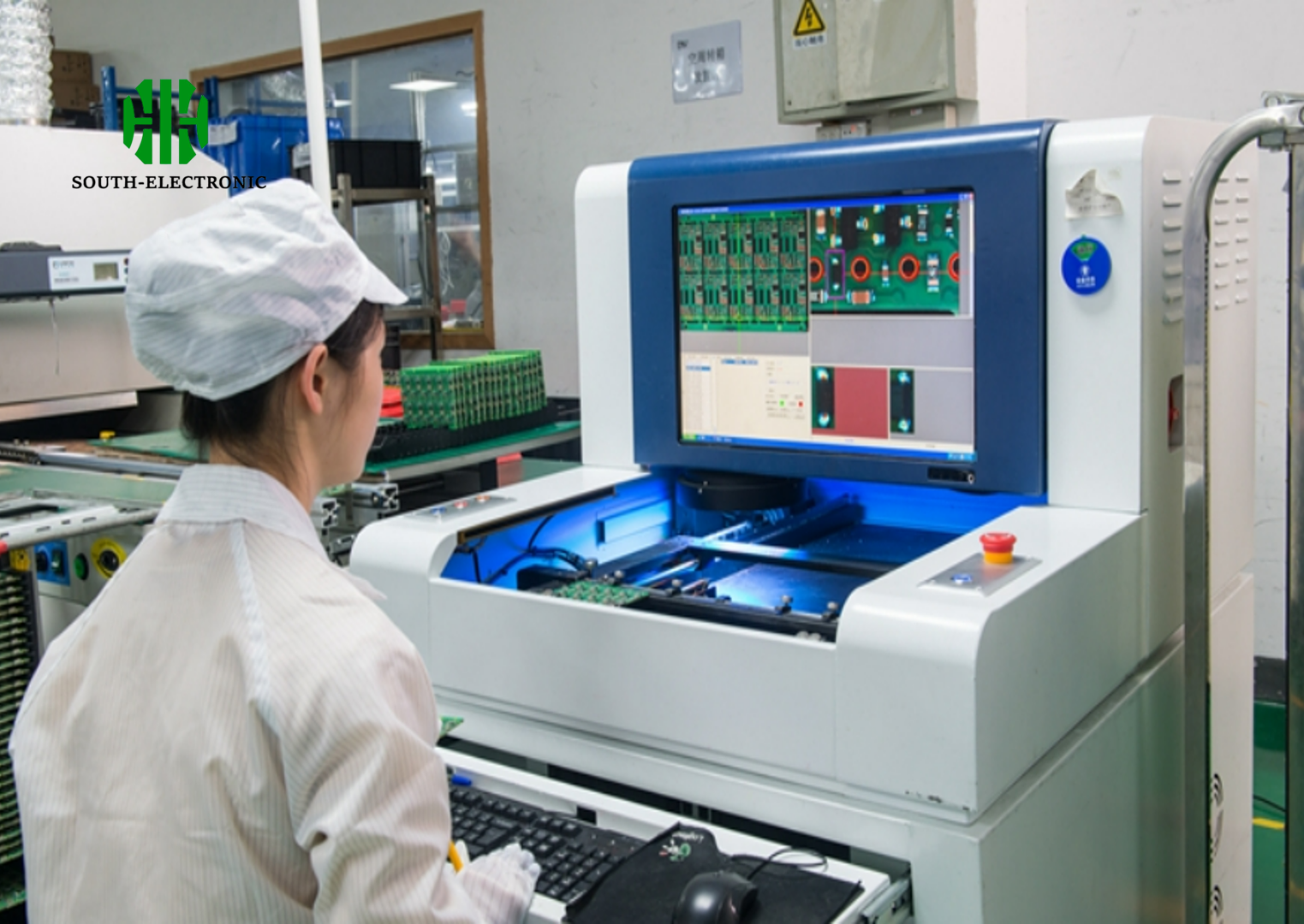
مراقبة الجودة واختبار لوحات الدوائر المطبوعة عالية الكثافة
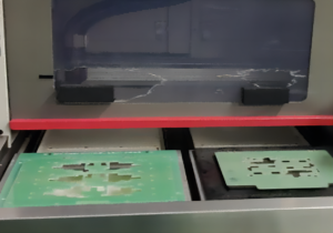
تعد مراقبة الجودة واختبار لوحات HDI جوانب حاسمة في إنتاج لوحات الدوائر المطبوعة عالية الكثافة، مما يضمن أن المنتج النهائي يلبي المعايير العالية المطلوبة للأداء، والموثوقية، والمتانة. نظرًا للتعقيد والكثافة في تصميمات HDI، من الضروري اتباع بروتوكولات اختبار صارمة لاكتشاف ومعالجة أي عيوب في وقت مبكر من عملية التصنيع. يساعد ذلك في منع الفشل المكلف ويضمن أن تعمل اللوحة كما هو مقصود في التطبيقات التي تتطلب أداءً عاليًا، مثل الاتصالات، الطيران، والأجهزة الطبية. فيما يلي عمليات مراقبة الجودة الأساسية وطرق الاختبار المستخدمة في إنتاج لوحات HDI.
عمليات مراقبة الجودة الأساسية في إنتاج لوحات HDI
يتضمن إنتاج لوحات HDI عدة مراحل، وكل مرحلة تتطلب مراقبة جودة صارمة للحفاظ على دقة واتساق عاليين. تشمل التدابير الرئيسية لمراقبة الجودة ما يلي:
- مراجعة التصميم للتصنيع (DFM): قبل بدء الإنتاج، تضمن مراجعة شاملة لتصميم DFM أن تصميم اللوحة الأمثل للتصنيع. تحدد هذه المراجعة أي عناصر تصميم قد تكون صعبة أو مكلفة للإنتاج، مما يساعد في منع تأخيرات الإنتاج أو الأخطاء.
- مراقبة الجودة أثناء العملية: خلال عملية التصنيع، تُجرى فحوصات الجودة في مراحل مختلفة لاكتشاف أي مشكلات قبل تفاقمها. تشمل هذه الفحوصات عمليات الحفر، والترقيق، والنقش، والتغطية بالنحاس للتأكد من أن الفتحات والآثار والطبقات محاذية بشكل صحيح وتلبي المواصفات المطلوبة.
- ضمان جودة المواد: يتم اختبار المواد المستخدمة في إنتاج لوحات HDI، مثل رقائق النحاس، والرقائق المعززة، والمواد العازلة، بعناية لضمان الجودة. يضمن ذلك أنها تلبي المعايير المطلوبة للأداء الكهربائي، والثبات الحراري، والقوة الميكانيكية. يعد ضمان الاتساق والجودة لهذه المواد أمرًا حاسمًا لتجنب مشكلات مثل إزالة الترقيق أو عيوب الآثار.
أنواع الاختبارات
يتم استخدام عدة طرق اختبار متقدمة في تصنيع لوحات HDI للتحقق من الوظائف، واكتشاف العيوب، وضمان الجودة العامة. تشمل بعض تقنيات الاختبار الأكثر استخدامًا:
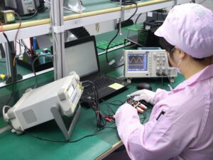
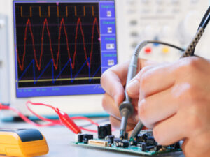
- الاختبار الكهربائي (ET): يضمن الاختبار الكهربائي أن لوحات HDI تعمل كما هو متوقع عن طريق التحقق من استمرارية جميع التوصيلات الكهربائية واكتشاف أي دوائر قصيرة، أو دوائر مفتوحة، أو مشكلات كهربائية أخرى. غالبًا ما يتم استخدام اختبار “التحقيق الطائر” أو “سرير المسامير” لاستكشاف كل شبكة على اللوحة، مما يضمن توصيل جميع الآثار والفتحات بشكل صحيح وعملها بدون أخطاء. بالنسبة للوحات HDI، التي تحتوي عادةً على تصميمات معقدة وكثيفة، يعتبر هذا النوع من الاختبارات حيويًا للتأكد من تكوين جميع التوصيلات عالية الكثافة بشكل صحيح.
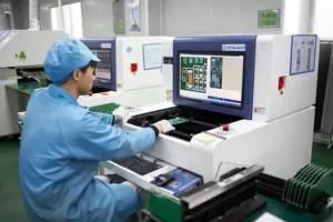
- الفحص البصري الآلي (AOI): يستخدم AOI كاميرات عالية الدقة لفحص سطح اللوحة تلقائيًا لاكتشاف العيوب مثل المكونات غير المحاذية، عرض الآثار غير الصحيح، المكونات المفقودة أو الخاطئة، وغيرها من الشذوذ البصري. في لوحات HDI، حيث تكون عرض الآثار والتباعد ضئيلة جدًا، يكون AOI مفيدًا بشكل خاص في اكتشاف العيوب التي قد لا تكون مرئية للعين المجردة. تستخدم أنظمة AOI خوارزميات التعرف على الأنماط لمقارنة اللوحة الفعلية بملفات التصميم الأصلية، وتحديد أي اختلافات.
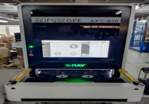
- الفحص بالأشعة السينية: يعتبر الفحص بالأشعة السينية مهمًا بشكل خاص للوحات HDI، حيث تكون العديد من ميزاتها، مثل الفتحات المدفونة والمكدسة، مخفية تحت طبقات المواد ولا يمكن فحصها باستخدام الطرق البصرية. يسمح اختبار الأشعة السينية للمصنعين برؤية داخل طبقات اللوحة والتحقق من سلامة هذه التوصيلات المخفية. يُستخدم عادةً لفحص الفراغات في الفتحات، وسوء محاذاة الطبقات، وأي عيوب داخلية يمكن أن تؤثر على موثوقية اللوحة.
- اختبار قابلية اللحام: يضمن أن تشطيب سطح اللوحة HDI، مثل ENIG (نيكل غامر ذاتي التحفيز بذهب) أو OSP (مادة حافظة عضوية للحام)، يوفر قابلية لحام مناسبة لتركيب المكونات. يمكن أن تؤدي قابلية اللحام السيئة إلى وصلات لحام ضعيفة، مما يسبب مشكلات في الأداء أو فشلًا.
- اختبار الإجهاد الحراري والتدوير الحراري: غالبًا ما تخضع لوحات HDI لتدوير حراري لمحاكاة تغيرات درجة الحرارة التي ستتعرض لها في التطبيقات الواقعية. يساعد هذا الاختبار في تحديد أي مشكلات محتملة تتعلق بالتمدد والانكماش الحراري، والتي قد تتسبب في تشقق الفتحات أو إزالة الترقيق. يتم أيضًا إجراء اختبار الإجهاد الميكانيكي لتقييم قدرة اللوحة على تحمل الإجهاد الفيزيائي، مثل الانحناء أو الاهتزاز، دون التأثير على الأداء.
كيفية ضمان موثوقية ومتانة لوحات HDI
نظرًا للتطبيقات الحرجة للوحات HDI، يعد ضمان موثوقيتها ومتانتها أمرًا ضروريًا. يستخدم المصنعون عدة تقنيات لتحسين عمر اللوحات وتقليل خطر الفشل أثناء التشغيل:
- المواد عالية الجودة: يمكن أن يؤدي استخدام مواد عالية الجودة مثل البوليميد، والرقائق المعززة عالية الأداء، وطبقات النحاس السميكة إلى تحسين متانة اللوحات، خاصة في البيئات القاسية حيث يكون الإجهاد الحراري والميكانيكي شائعًا.
- سلامة الفتحات: يعد ضمان التكوين الصحيح للفتحات أمرًا بالغ الأهمية لموثوقية لوحات HDI. تساعد عمليات ملء الفتحات وتغطيتها بالنحاس على تحسين القوة الميكانيكية للمايكروفياس، مما يمنع التشققات أو الفشل أثناء التدوير الحراري أو الاهتزاز.
- تصميم إدارة الحرارة: تميل لوحات HDI التي تحتوي على مكونات كثيفة إلى تراكم الحرارة، مما قد يؤدي إلى تدهور الأداء بمرور الوقت.
- اختبارات بيئية: تخضع لوحات HDI المصممة للتطبيقات الحرجة، مثل الطيران، والسيارات، والأجهزة الطبية، لاختبارات بيئية تتعرض فيها لدرجات حرارة قصوى، رطوبة، وأجواء تآكلية.
باختصار، تعد مراقبة الجودة والاختبار أساسية لضمان الوظيفة، الموثوقية، والمتانة للوحات HDI. باستخدام طرق اختبار صارمة مثل الاختبار الكهربائي، AOI، وفحص الأشعة السينية، والالتزام بمعايير مراقبة الجودة الصارمة، يمكن للمصنعين توفير لوحات HDI تفي بمطالب الأداء العالي للأجهزة الإلكترونية الحديثة.
الفصل 8
اعتبارات التكلفة للوحات الدوائر المطبوعة عالية الكثافة
عندما تخطط لإنتاج لوحات HDI، يجب أن تأخذ التكلفة بعين الاعتبار. يمكن أن تختلف التكلفة حسب تعقيد التصميم، المواد المستخدمة، وعمليات التصنيع التي تمر بها. إذا فهمت هذه العوامل المؤثرة في التكلفة، يمكنك اتخاذ قرارات مدروسة حول كيفية موازنة التكلفة والجودة.
العوامل التي تؤثر على تكلفة لوحات HDI
تعتمد تكلفة لوحات HDI على عدة عوامل، معظمها يتعلق بتعقيد التصميم والعمليات المطلوبة للتصنيع. إليك بعض العوامل الرئيسية التي تؤثر على التكلفة:
- عدد الطبقات: كلما زاد عدد الطبقات في لوحة HDI، زادت تكلفة الإنتاج. وذلك لأن محاذاة وتغليف الطبقات المتعددة أكثر تعقيدًا، وتتطلب المزيد من المواد والعمالة.
- تقنية الفتحات: يؤثر نوع وعدد الفتحات المستخدمة على التكلفة. تتطلب المايكروفياس، والفتحات العمياء، والمدفونة عمليات متقدمة مثل الحفر بالليزر والتغليف الدقيق.
- المواد: تكلفة المواد عالية الجودة مثل البوليميد، والرقائق المملوءة بالسيراميك، أو الركائز عالية الحرارة تكون أعلى. وتكون هذه المواد ضرورية للتطبيقات التي تحتاج إلى استقرار حراري عالي، مرونة، أو متانة، مثل الطيران، والأجهزة الطبية.
كيفية تحقيق التوازن بين التكلفة والجودة عند شراء لوحات HDI
يجب إيجاد التوازن الصحيح بين التكلفة والجودة عند شراء لوحات HDI. إليك بعض النصائح لتحقيق التوازن المطلوب:
- التعاون مع المصنع: تحدث مع المصنعين قبل بدء التصنيع. يمكنهم مساعدتك في تصميم اللوحات بطريقة تسهل التصنيع وتخفض التكاليف.
- التصميم الصحيح: احرص على تصميم لوحات HDI بشكل صحيح لتوفير التكلفة.
- اختر موردًا جيدًا: تأكد من اختيار مورد لديه خبرة في تصنيع لوحات HDI ومعتمد بمعايير الجودة.
الخلاصة
على الرغم من أن لوحات HDI قد تكون مكلفة في البداية، إلا أنها توفر المال على المدى الطويل بسبب موثوقيتها وحجمها الصغير وملاءمتها للإنتاج بالجملة.
الفصل 9
مزايا لوحات الدوائر المطبوعة عالية الكثافة مقارنة بلوحات الدوائر التقليدية
تتفوق لوحات HDI (High-Density Interconnect) على لوحات الدوائر التقليدية بعدة طرق، خاصةً عندما تحتاج إلى أداء أعلى، حجم أصغر، وموثوقية أكبر.
- مزيد من المكونات: تتيح لك لوحات HDI وضع المزيد من المكونات في مساحة أصغر باستخدام المايكروفياس، الفتحات العمياء والمدفونة، مما يمكنك من إنشاء تصميمات أكثر تعقيدًا وضغطًا مقارنةً بلوحات الدوائر العادية. هذا مهم جدًا للأجهزة ذات المساحة المحدودة.
- أصغر حجم: تمكنك لوحات HDI من تصميم لوحات أصغر وأخف وزنًا، وهو أمر ضروري في الهواتف الذكية، الأجهزة القابلة للارتداء، وقطاع الطيران، حيث يكون الحجم والوزن أمرين مهمين.
- إشارات أفضل: توفر لوحات HDI إشارات أفضل بفضل وجود عدد أقل من المسارات للإشارات، مما يقلل من التداخل الكهرومغناطيسي (EMI) وتداخل الإشارات (crosstalk). هذا مهم جدًا للتطبيقات عالية السرعة مثل 5G، مراكز البيانات، والاتصالات.
- تحسين في التبديد الحراري: تتيح لوحات HDI التخلص من الحرارة بشكل أفضل بفضل الفتحات الحرارية والتصميم المحسن، مما يقلل من ارتفاع درجات الحرارة ويطيل عمرها في التطبيقات ذات القدرة العالية.
- موثوقية أكبر: تعد لوحات HDI أكثر موثوقية لأنها تحتوي على فتحات مكدسة ومواد ذات جودة أعلى، مما يقلل من احتمالية تعرضها للتلف في السيارات، الطائرات، والقطاع العسكري.
- سرعة أعلى: تسمح لوحات HDI بسرعة أعلى حيث لا تحتاج الإشارات للمرور لمسافات طويلة، مما يجعلها مثالية للاتصالات، الشبكات، وأجهزة الكمبيوتر السريعة.
- خيارات أكثر: توفر لوحات HDI المزيد من الخيارات بفضل إمكانية تكديس المزيد من الطبقات والقيام بالمزيد باستخدام الفتحات، مما يتيح تصميمات أكثر تعقيدًا ومرونة، مثل الأجهزة الطبية والاستهلاكية.
- أقل تكلفة على المدى الطويل: تكون لوحات HDI أغلى في البداية، ولكنها تصبح أقل تكلفة مع الإنتاج الضخم حيث يمكن تصنيعها بشكل أسرع ووضع المزيد من المكونات في لوحة واحدة، مما يوفر المال في النظام الكامل.
باختصار، تعد لوحات HDI أفضل لأنها أصغر، أسرع، وأكثر موثوقية، ويمكن استخدامها في مجموعة متنوعة من المجالات مثل الاتصالات، الطيران، السيارات، والاستهلاك.
الفصل 10
مستقبل تقنية لوحات الدوائر المطبوعة عالية الكثافة
مع استمرار تطور التكنولوجيا، ستصبح لوحات HDI أصغر وأسرع وأكثر قوة. إليك بعض الاتجاهات التي نتوقع رؤيتها:
- تطور تقنية HDI: تصبح لوحات HDI أكثر تعقيدًا، مع تصميمات متعددة المراحل، وتغليف ثلاثي الأبعاد، وتقنية النظام في الحزمة (SiP). يسمح لنا هذا بتعبئة المزيد من المكونات في مساحة أصغر والحصول على أداء أفضل.
- مواد وتقنيات جديدة: بدأنا في استخدام مواد جديدة مثل الركائز المرنة والرقائق عالية التردد (مثل PTFE). كما نستخدم تقنيات جديدة مثل التصوير بالليزر المباشر (LDI) وتقنيات الفتحات المتقدمة. هذه التقنيات تتيح لنا إنشاء آثار أصغر، إدارة الحرارة بشكل أفضل، وتعبئة المزيد من المكونات في مساحة أصغر.
- لوحات HDI وإنترنت الأشياء (IoT) والذكاء الاصطناعي (AI) وشبكات 5G: ستكون لوحات HDI مهمة للغاية لأجهزة IoT لأنها تحتاج إلى أن تكون صغيرة وتستهلك طاقة أقل. كما ستكون مهمة لأنظمة الذكاء الاصطناعي وحوسبة الأطراف لأنها تحتاج إلى معالجة البيانات بسرعة كبيرة. وستكون مهمة لشبكات 5G لأنها تستطيع التعامل مع الإشارات عالية التردد وجعل محطات القاعدة أصغر.
- لوحات HDI وتغليف أشباه الموصلات: ستبدأ لوحات HDI في العمل مع أنواع جديدة من تغليف أشباه الموصلات، مثل التغليف عند مستوى الرقاقة (FO-WLP) وتقنية النظام في الحزمة (SiP). سيسمح لنا هذا بتصنيع أجهزة أصغر وأسرع.
- الاستدامة: نحن نهتم أكثر بالبيئة، لذا نستخدم لحام خالٍ من الرصاص، رقائق خالية من الهالوجين، ومواد قابلة لإعادة التدوير. نريد التأكد من أننا لا نضر بالكوكب.
بالتالي، ستستمر لوحات HDI في دعم ثورات إنترنت الأشياء، الذكاء الاصطناعي، وشبكات 5G. وستواصل التطور بمواد جديدة، تغليف حديث، وطرق جديدة للحفاظ على البيئة.
تواصل معنا
أين نحن؟
الحديقة الصناعية، رقم 438 شارع دونغ هوان، رقم 438، شاجينغ دونغ هوان، منطقة باوان، شنتشن، قوانغدونغ، الصين
الطابق 4، مبنى زهيهوي الإبداعي، رقم 2005 شارع شيهوان، شاجينغ، منطقة باوان، شنتشن، الصين
الغرفة A1-13، الطابق 3، مركز يي ليم الصناعي، 2-28 شارع كواي لوك، كواي تشونغ، هونغ كونغ
service@southelectronicpcb.com
الهاتف: +86 400 878 3488
أرسل لنا رسالة
كلما كانت التفاصيل أكثر دقة، كلما تمكنا من المضي قدمًا إلى الخطوة التالية أسرع.

