
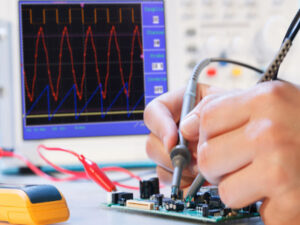
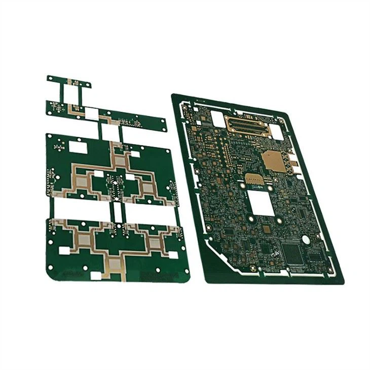
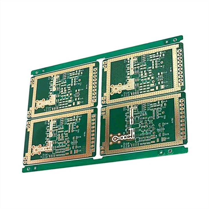
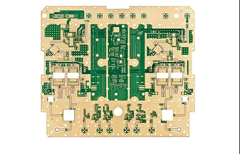
حل تصميم لوحة الدائرة المطبوعة بتردد عالي
South-Electronic
South-Electronic هي مصدرك الأمثل للوحات الدائرة المطبوعة بتردد عالي عالية الجودة وموثوقة وذات قيمة عالية. استفد من خدمة تصميم لوحة الدائرة المطبوعة بتردد عالي الشامل لدينا - من المفاهيم إلى الاكتمال، نقدم ضمانًا للدقة والموثوقية والالتزام الصارم بمعايير الصناعة.
لماذا تختار South-Electronic؟
-
الدقة والجودة
في South-Electronic، نقوم بالتأكد من الدقة والموثوقية في كل لوحة دائرة مطبوعة بتردد عالي ننتجها، مما يضمن أن تكون منتجاتك خالية من العيوب وتعمل بالضبط كما هو متوقع.
-
التخصيص المرن
نقوم بتكييف خدماتنا لتلبية متطلباتك المحددة، سواء كنت بحاجة إلى تجميع جانبي واحد أو جانبيين أو تجميع BGA. مهما كانت احتياجاتك، يمكنك تسليم طلباتك بمرن، مع الحفاظ على جودة لا تشوبها شائبة.
-
إيقاف سريع
نحن نفهم أن الوقت أمر بالغ الأهمية لعملك. لذلك، تضمن خطوط الإنتاج الكفؤة لدينا أن تتلقى طلباتك بسرعة، مما يساعدك على البقاء في صدارة مواعيدك وحدودك الزمنية وتحقيق مشاريعك.
-
فريق محترف
عندما تعمل معنا، ستتم دعمك من قبل فريق لديه سنوات من الخبرة في تجميع لوحة الدائرة المطبوعة. سوف تستفيد من ثقة العمل مع محترفين يفهمون ngànhك ويعرفون كيفية تلبية احتياجاتك المحددة.
-
حل شامل
من التصميم الأولي إلى التجميع النهائي، نقوم بإدارة كل خطوة في العملية. معنا، تحصل على ميزة شريك خدمي كامل يمكنه التعامل مع جميع احتياجات لوحة الدائرة المطبوعة بشكل متماسك، مما يمنحك راحة البال وتيسير سير عملك.
-
لا توجد متطلبات量 أدنى للطلب
لديك حرية طلب ما تحتاجه بالضبط، مهما كانت الكمية صغيرة. حتى لو كان الأمر يتعلق بوحدة واحدة، نحن هنا لتلبية متطلباتك دون أي قيود للمجموع الأدنى للطلب، مما يعطيك مرونة كاملة في قرارات الشراء الخاصة بك.
المشروع المرتبط الذي قمنا ب انجازه
تعليقات العملاء
الأسئلة الشائعة
الأسئلة الأكثر شيوعًا
أرسل لنا رسالة


دليل كامل لتصميم لوحة الدائرة المطبوعة بتردد عالي
المحتوى
الفصل 1
مدخل إلى لوحات الدائرة المطبوعة ذات التردد العالي
ما هي لوحات الدائرة المطبوعة ذات التردد العالي؟
لوحات الدائرة المطبوعة ذات التردد العالي ليست مجرد لوحات دائرة قديمة؛ بل هي مصممة خصيصًا لتتفوق في البيئات التي يتطلب فيها نقل إشارات سريع وموثوق. عادةً ما يتم изготовع هذه اللوحات من مواد تتميز بخسارة عازلة منخفضة، مثل FR-4 أو بولي تترا فلورو إيثيلين (PTFE)، مما يساعد على الحفاظ على صحة الإشارة حتى عند سرعات عالية. هذا يعني أنها يمكنها التعامل مع التبديل السريع لتشغيل وإيقاف الإشارات الرقمية ونقل الإشارات التناظرية بشكل سلس عبر أجهزة إلكترونية مختلفة.
لماذا لوحات الدائرة المطبوعة ذات التردد العالي مهمة جدًا؟
في عالم اليوم الذي يتمحور حول التكنولوجيا، لا يمكن التقليل من أهمية لوحات الدائرة المطبوعة ذات التردد العالي. إنها العمود الفقري للعديد من التطبيقات التي تعتمد عليها كل يوم. من أنظمة WiFi و GPS في هاتفك الذكي إلى أنظمة أكثر تعقيدًا مثل الرادار وأجهزة الاتصالات الفضائية، تعمل هذه اللوحات على ضمان تشغيل الأجهزة بدقة وسرعة مطلوبة في عصر 数ي عالي المخاطر.
علاوة على ذلك، مع استمرار الطلب على أجهزة إلكترونية أسرع وأكثر موثوقية، تصبح دور لوحات الدائرة المطبوعة ذات التردد العالي أكثر حاسمية. إنها مفتاح الابتكار في الاتصالات السلكية واللاسلكية والدفاع والفضاء والالكترونيات الاستهلاكية، حيث تساهم في تقدم التكنولوجيا الذي يدفع بالحدود مما هو ممكن.
من خلال اختيار لوحات الدائرة المطبوعة ذات التردد العالي، لا تقوم بただ اختيار الأداء الإلكتروني الأفضل؛ بل=tkh tambiénاستثمار في مستقبل التكنولوجيا. تقف هذه اللوحات في طليعة الإلكترونيات الحديثة، وتدفع بالتقدّم في العديد من الصناعات من خلال تمكين الاتصالات الإلكترونية الأسرع والموثوقة والأكثر كفاءة. سواء كنت تقوم بتطوير إلكترونيات استهلاكية متقدمة أو أنظمة فضائية متطورة، توفر لوحات الدائرة المطبوعة ذات التردد العالي القدرات التي تحتاجها للنجاح في المنظر التكنولوجي السريع الذي نعيشه اليوم.
الفصل 2
مواد وسبل للطوابع الدقيقة عالية التردد
عندما تدخل في تصميم الطوابع الدقيقة عالية التردد، يصبح اختيار المواد والسبل أمرًا حرجًا. أداء الطوابع الدقيقة الخاصة بك عند الترددات العالية يعتمد على هذه المكونات الأساسية. اختيار المواد المناسبة ليس فقط لتأمين الوظائف، بل لتعظيم الكفاءة وسلامة الإشارات وأداء الأجهزة الإلكترونية بشكل عام.
ما هي المواد المستخدمة في الطوابع الدقيقة عالية التردد؟
الطوابع الدقيقة عالية التردد تتطلب مواد ذات خصائص كهربائية استثنائية لمعالجة انتشار الإشارات السريعة دون خسائر كبيرة. هنا بعض المواد الأكثر شيوعًا المستخدمة في الطوابع الدقيقة عالية التردد:
- PTFE (بоли تترافلورو إيثيلين): المعروف بمسمى العلامة التجارية مثل تيفلون، PTFE извест برای ثابت عزل منخفض وعامل التبديد المنخفض، والتي هي مهمة لتقليل فقدان الإشارات عند الترددات العالية. إنه المادة المفضلة للتطبيقات التي تتطلب أداء ميكروويف ممتازًا.
- FR-4: بينما FR-4 القياسي هو مادة شائعة للتطبيقات منخفضة التردد، هناك درجات FR-4 عالية الأداء متاحة التي تقدم خصائص عزل محسنة للتطبيقات عالية التردد معتدلة. هذا يجعل FR-4 خيارًا ekonomikًا عندما لا تكون الأداء القصوى مطلوبة.
- مواد روجرز: هذه السبل مصممة خصيصًا للطوابع الدقيقة عالية التردد. مواد روجرز مثل RO4003C وRO4350B توفر خسائر عزل منخفضة ومراقبة معاوقة أفضل وأداء حراري، مما يجعلها مثالية للتطبيقات المتطلبة في صناعات الفضاء والاتصالات السلكية والسيارات.
- م イ: للامينيتات المحشوة بالسيراميك: هذه السبل تتضمن حشوات سيراميكية لتحسين التوصيل الحراري وتقليل التمدد الحراري، والذي هو مهم ل الحفاظ على السلامة الهيكلية وثبات الأداء للطوابع الدقيقة عند الترددات العالية.
كيف تؤثر هذه المواد على سلامة الإشارات والأداء؟
اختيار مادة السبلا يؤثر بشكل مباشر على سلامة الإشارات الخاصة بالطوابع الدقيقة عالية التردد بعدة طرق:
- ثابت العزل (Dk): ثابت عزل منخفض يساعد في تقليل تأخير الإشارات. المواد مثل PTFE لها ثابت عزل منخفض، والتي تكون مفضلة لنقل الإشارات عالية التردد لأنها تسمح بسرعة إشارة أسرع مع تباين معاوقة أقل.
- عامل التبديد: يُعرف أيضًا باسم زاوية الفقد، هذا العامل يقيس كمية الطاقة الكهرومغناطيسية المفقودة بسبب الخصائص الذاتية لمادة السبلا. المواد ذات عوامل تبديد منخفضة، مثل روجرز وPTFE، هي مهمة في تقليل خسائر الطاقة في التطبيقات عالية التردد.
- إدارة الحرارة: العمليات عالية التردد يمكن أن تولد حرارة كبيرة. المواد مثل لامينات السيراميك المحشوة مهمة لأنها ت散ع الحرارة بشكل أكثر فعالية، مما يحافظ على سلامة الدائرة وأدائها مع مرور الوقت.
- الاستقرار البعدي: المواد مثل روجرز ولامينات السيراميك المحشوة تظهر استقرارًا بعديًا متفوقًا تحت الإجهاد الحراري، والذي هو مهم ل الحفاظ على التolerances الضيقة في الدوائر عالية التردد.
اختيار المواد المناسبة للطوابع الدقيقة الخاصة بك عالية التردد ليس مجرد удовлетворение المتطلبات الدنيا؛ إنه حول تعزيز الأداء والموثوقية لمنتجك النهائي. каждая مادة تظهر مجموعة من الخصائص التي يمكن أن تزيد أو تعيق فعالية التصاميم الخاصة بالطوابع الدقيقة عالية التردد، مما يؤثر على كل شيء من سرعة الإشارة ووضوحها إلى إدارة الحرارة والاستقرار الميكانيكي. لذلك، فهم واختيار السبلا المثالية هو قرار حرج يمكن أن يحدد نجاح التطبيقات الإلكترونية الخاصة بك عالية التردد.
الفصل 3

اعتبارات التصميم للوحة الدوائر المطبوعة عالية التردد
تصميم عالية التردد PCBs هو فن يجمع بين الهندسة المتقدمة مع التنفيذ الدقيق. عندما تدخل عالم تصميم высок التردد PCB ، كل quyết định تقوم بها من التصميم إلى اختيار المواد له تأثير على أداء وموثوقية المنتج النهائي. دعونا نغوص في العوامل الرئيسية للتصميم والتقنيات التي تحظى بأهمية حاسمة لتحسين التطبيقات عالية التردد.
العوامل الرئيسية للتصميم ل عالية التردد PCBs
- اختيار المواد: كما ناقشنا ، اختيار المواد هو أساسي. لتطبيقات عالية التردد ، تحتاج إلى مواد ذات ثوابت عازلة منخفضة وذات خسائر منخفضة لتجديد سلامة الإشارة. يجب أن تكون المواد مثل PTFE (Teflon) و Rogers واللامينات المملئة بالسيراميك في قائمة الأولويات. هذه المواد لا تدعم فقط الترددات الأعلى ولكنها också تحد من خسائر الإشارة ، مما يوفر قاعدة قوية لتصاميمك.
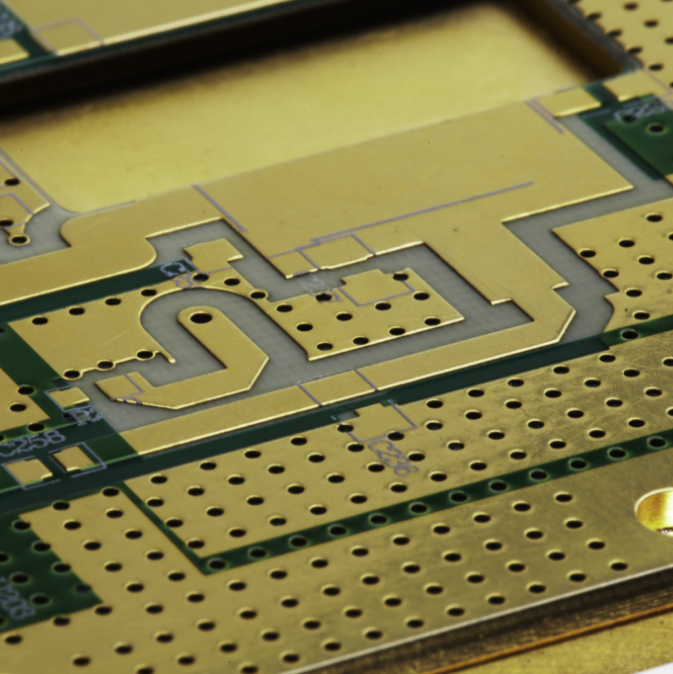
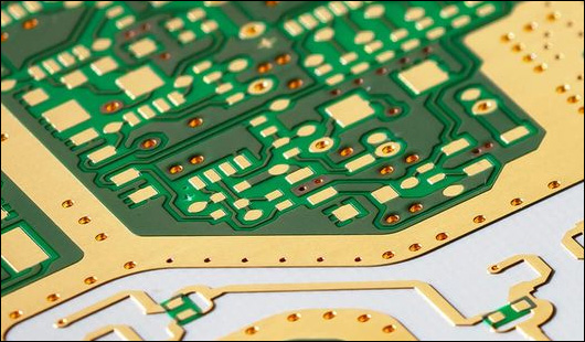
- مراقبة.Impedance: في عالية التردد PCBs ، مراقبة الـ impedance هي أمر بالغ الأهمية لمنع انعكاس الإشارة و خسائر النقل. يتضمن ذلك حسابات دقيقة وتعديلات على عرض وفترات التتبع ، استنادًا إلى الخصائص العازلة للطبقة العازلة. تحقيق الـ impedance المتسق يتطلب ممارسات تصميم دقيقة وغالبًا ما يتطلب сотрудارة مع موردي المواد لضمان مراعاة المواصفات.
- هندسة التتبع: شكل وتصميم التتبع له تأثير كبير على الأداء. استخدم تتبعات منحنية ناعمة بدلاً من التتبعات الزاوية لتقليل انعكاس الإشارة وتداخل الإشارات. بالإضافة إلى ذلك ، يجب تحسين سمك التتبع لتحقيق توازن بين المقاومة والحث والسعة ، مما هو ضروري لصون سلامة الإشارة عند الترددات العالية.
التقنيات لتقليل خسارة الإشارة و تحسين الموثوقية
- استخدام طائرات الأرض: تنفيذ طائرات أرض صلبة تحت طبقات الإشارة يمكن أن يقلل بشكل كبير من تداخل الإشارات الكهرومغناطيسية (EMI) و يوفّر مستوى جهد مرجعي مستقر ، وهو أمر ضروري لصون سلامة الإشارة. طائرات الأرض تساعد أيضًا في تبديد الحرارة ، مما يضيف إلى موثوقية اللوحة.
- التحويط والتتبع الحارس: لتحسين حماية ضد EMI والضوضاء الخارجية ، فكر في استخدام تقنيات التحويط. يمكن دمج التحويط المعدني فوق المناطق الحساسة من اللوحة. بالإضافة إلى ذلك ، يمكن استخدام تتبعات حارس مع vias متصلة بالأرض حول تتبعات التردد العالي لفصلها عن مكونات الدائرة الأخرى.
- إدارة الحرارة: الترددات العالية يمكن أن تؤدي إلى أحمال حرارية متزايدة ، لذلك إدارة الحرارة الفعالة أمر بالغ الأهمية. صمم PCBs مع وحدات تخفيف حراري و وحدات تبريد إذا لزم الأمر. بالإضافة إلى ذلك ، اختيار المواد ذات التوصيل الحراري الجيد يمكن أن يساعد في تبديد الحرارة بكفاءة أكبر ، مما يحافظ على سلامة وطول عمر الدائرة.
- تصميم الفياس: في عالية التردد PCBs ، يلعب تصميم الفياس دورًا هامًا. استخدم فياس عمياء ومدفونة لتقليل مسار نقل الإشارة ، وبالتالي تقليل تدهور الإشارة. يجب التخطيط بعناية لوضع وحجم الفياس لتجنب انقطاع الـ impedance.
- تركيب المكونات: تركيب المكونات الاستراتيجي أمر ضروري لتقليل أطوال المسار للإشارات الحرجة ، وبالتالي تقليل فرص خسارة الإشارة والتداخل. يجب ترتيب المكونات لتحسين تدفق الإشارة وتقليل عبور مسارات التردد العالي ، مما يمكن أن يIntroduced ضوضاء وخسارة.
- التجربة وتصنيع النماذج: قم دائمًا بتصنيع نماذج لتصاميمك قبل الإنتاج الكامل. تجربة نماذجك تسمح لك بالتعرف على ومعالجة مشاكل تتعلق بسلامة الإشارة والوظائف. هذا الخطوة هو أمر بالغ الأهمية لضمان أن تصميمك لا يلتزم فقط بالمواصفات المطلوبة ولكن أيضًا يعمل بشكل موثوق في التطبيقات الواقعية.
من خلال مراعاة هذه العوامل للتصميم و توظيف هذه التقنيات ، يمكنك تحسين أداء وموثوقية عالية التردد PCBs بشكل كبير. كل تصمیم في عملية التصميم هو خطوة نحو تحقيق منتج لا يلتزم فقط بالطلبات الصارمة للتطبيقات عالية التردد بل يتجاوزها أيضًا.
الفصل 4
السلامة وادارة الاشارة
عندما تقوم بتصميم لوحات الدائرة المطبوعة عالية التردد ، فإنك تواجه تحدي الحفاظ على سلامة الإشارة. سلامة الإشارة هي عصب الحياة لأجهزتك الإلكترونية. إنها ما يضمن أن الإشارات التي ترسلها عبر لوحة الدائرة المطبوعة لا تتأثر أو تتقطع. انتقالك إلى ترددات أعلى ، تصبح سلامة الإشارة أكثر أهمية وصعوبة في الإدارة. دعونا نتحدث عن بعض التحديات وأفضل الممارسات للحفاظ على سلامة الإشارة بحيث تعمل أجهزتك بالطريقة التي من المفترض أن تعمل بها.
التحديات في الحفاظ على سلامة الإشارة عند الترددات العالية
- تقليل الإشارة: زيادة التردد ، يصبح فقدان الإشارة أكثر وضوحًا بسبب الخواص المحددة للمواد وتصميم لوحة الدائرة المطبوعة. هذا يمكن أن يؤدي إلى إشارات أضعف في نهاية المستلم ، مما يؤثر على الأداء العام لجهازك الإلكتروني.
- انعكاس الإشارة وتداخل الإشارات: عدم مطابقة.Impedance وترaces المزدحمة يمكن أن يؤدي إلى انعكاس الإشارة وتداخل الإشارات بين القنوات. هذه الظواهر لا تؤثر فقط على جودة الإشارة ولكن يمكن أن تسبب أيضًا تلف البيانات وفقدان المعلومات.
- التداخل الكهرومغناطيسي (EMI): الدوائر عالية التردد أكثر عرضة للمصادر الخارجية والداخلية للضوضاء ، والتي يمكن أن تؤدي إلى إشارات غير مرغوب فيها وتعطل العمليات العادية. إدارة EMI أمر بالغ الأهمية للحفاظ على سلامة إشارات التردد العالي.
الحلول وأفضل الممارسات لإدارة سلامة الإشارة
- اختيار المواد بدقة: اختيار المادة الشبكية الصحيحة هو خط الدفاع الأول عن سلامة الإشارة. المواد ذات الثوابت العازلة المنخفضة وعوامل التبديد المنخفضة ، مثل مادة PTFE أو Rogers ، مثالية لأنها تقلل من فقدان الإشارة وتدعم نقل الإشارات بسرعات أعلى.
- تحكم.Impedance: الحفاظ على.Impedance المتجانسة في جميع أنحاء لوحة الدائرة المطبوعة أمر بالغ الأهمية. هذا يتضمن تصميم hìnhometries و مواد عازلة محكمة لمطابقة.Impedance للمصدر والحمل. استخدم حاسبات.Impedance وبرمجيات المحاكاة لتحديد وضبط التصاميم لأداء مثالي.
- توجيه الإشارات الاستراتيجي: تقليل تداخل الإشارات وانعكاسها عن طريق توجيه إشارات التردد العالي الحاسمة على طبقات منفصلة أو استخدام إشارات محمية. استخدم التمييز التفاضلي حيث إن ذلك يساعد على إلغاء الضوضاء وتحسين سلامة الإشارة.
- استخدام الطائرات الأرضية: أدرج طائرات أرضية صلبة ومتواصلة في تصميم لوحة الدائرة المطبوعة. الطائرات الأرضية تقلل من مساحة الدائرة وتوفر مسارًا عائدًا للتيار ، مما يقلل بشكل كبير من مخاطر EMI وانعكاس الإشارة.
- فك الارتباط والترشيح: وضع مكثفات فك الارتباط بالقرب من دبابيس الطاقة لمكونات نشطة لتثبيت تقلبات إمداد الطاقة وتقليل الضوضاء. بالإضافة إلى ذلك ، استخدم تقنيات الترشيح لإزالة مكونات التردد العالي غير المرغوب فيها من إشاراتك.
- اختبارات متقدمة ومحاكاة: استفد من أدوات المحاكاة المتقدمة لتنبؤ وتحليل سلوك الإشارة قبل إنشاء نموذج مادي. يمكن أن تساعد المحاكاة في تحديد مشاكل محتملة مثل آثار EMI وعدم مطابقة.Impedance وانعكاس الإشارة ، مما يسمح لك بإجراء التعديلات الضرورية في وقت مبكر من عملية التصميم.
- المراجعة المنتظمة والتصميم التكراري: اعتمد ممارسة المراجعة التصميمية المنتظمة والتحسينات التكرارية. تقييم تصميمك في مراحل مختلفة يتيح لك تحديد ومعالجة القضايا المتعلقة بسلامة الإشارة ، مما يعزز موثوقية وأداء المنتج النهائي.
من خلال فهم هذه التحديات وتطبيق هذه أفضل الممارسات ، يمكنك تحسين سلامة إشارات لوحات الدائرة المطبوعة عالية التردد بشكل كبير. تذكر ، كل قرار تصميم تقوم به – من اختيار المواد إلى توجيه الإشارات – يؤثر على أداء منتجك في التطبيقات العملية الحقيقية. ضمان سلامة الإشارة المثالية ليس فقط عن الوفاء بالمواصفات الفنية ؛ إنه عن تقديم منتج يبرز لتحفة موثوقية وأداء متفوق.
الفصل 5
تركيب وتصميم الطبقات
عندما تدخل في تصميم لوحة الدائرة المطبوعة عالية التردد ، تحتاج إلى فهم مدى أهمية تركيب الطبقات وتصميمها. كيفية ترتيب طبقات لوحة الدائرة المطبوعة وتفاصيلها لا تؤثر فقط على عملية التصنيع ولكن أيضًا على أداء المنتج النهائي. دعونا ننظر كيف يمكن لتركيبات طبقات فعالة تحسين لوحات الدائرة المطبوعة عالية التردد والفوائد التي تقدمها.
لماذا تركيب الطبقات مهم؟
يُشير تركيب الطبقات إلى ترتيب طبقات النحاس والمواد العازلة في لوحة الدائرة المطبوعة. في التطبيقات عالية التردد ، تكون هذه التكوين مهمة لأنها تؤثر على كل شيء من سلامة الإشارة ومراقبة إلى إدارة الحرارةและการحاجز التداخل الكهرومغناطيسي (EMI). يضمن تركيب الطبقات المتأricht أن تنتقل الإشارات عالية التردد بفقدان واضطرابحد أدنى ، مما يجعله حجر زاوية في تصميم لوحة الدائرة المطبوعة الناجح.
استكشاف تكوينات طبقات فعالة
- تركيب الطبقات المتعددة القياسي: هذا هو تكوين شائع يتناوب بين طبقات الإشارة وأرضي. لوحات الدائرة المطبوعة عالية التردد ، من المهم وجود طبقات إشارة متقاربة مع طبقات أرضي لتقليل مساحات حلقات الإشارة وتقليل خطر EMI. يساعد ذلك في الحفاظ على انتقال الإشارة نظيفًا وتحسين التوافق الكهرومغناطيسي (EMC) بشكل عام.
- تركيب الطبقات المتماثل: يمكن أن يكون تركيب الطبقات المتماثل مفيدًا بشكل خاص في تصميمات الترددات العالية. هذا التكوين يعكس ترتيب الطبقات حول نواة مركزية ، مما يساعد على توازن هيكل لوحة الدائرة المطبوعة الكلية ، وتقليل الانحناء أثناء التصنيع ، والمحافظة على أداء كهربائي متسق في جميع أنحاء اللوحة.
- تركيب الطبقات ذو الكثافة العالية (HDI): يستخدم تقنية HDI مسافات وأPLICات أصغر ، وأقواس أصغر ، وتركيب مكونات أكثر كثافة. التطبيقات عالية التردد ، يمكن أن يقلل تركيب HDI من طول مسارات الإشارة ، مما يحسن سلامة الإشارة ويقلل من التحدث المتقاطع. بالإضافة إلى ذلك ، يسمح HDI بتصميمات أكثر ضيقًا ، مما هو في الأجهزة الإلكترونية الحديثة المحدودة بالمكان.
فوائد طرق تركيب مختلفة
- تحكم متقدم في : مع تخطيط طبقات متأricht بعناية ، يمكنك تحقيق تحكم دقيق في ، وهو أمر مهم لنقل إشارات التردد العالي. من خلال تكوين سمك وفراغ الطبقات بشكل مناسب ، يمكنك الحفاظ على مستويات Impedance متسقة في جميع أنحاء لوحة الدائرة المطبوعة ، مما يقلل من انعكاسات الإشارة والخسائر.
- سلامة إشارة محسّنة: تقلل تكوينات الطبقات الفعالة من احتمال التداخل وتوهين الإشارة. من خلال فصل طبقات الإشارة عالية السرعة عن مصادر الضوضاء المحتملة واستخدام طبقات أرضي كحاجز ، تضمن أن تبقى إشاراتك قوية وواضحة على طول مسارات النقل.
- إدارة حرارية أفضل: يمكن أن يؤثر تركيب الطبقات على كيفية توزيع الحرارة والامتصاص عبر لوحة الدائرة المطبوعة. من خلال وضع الطبقات الحرارية أو الطبقات الحاملة للحرارة بشكل استراتيجي ، يمكنك إدارة الحرارة الناتجة عن عمليات التردد العالي ، وحماية المكونات الحساسة ، وتحسين موثوقية اللوحة.
- زيادة المتانة والموثوقية: يساهم تركيب الطبقات المخطط له في استقرار لوحة الدائرة المطبوعة بدنيًا. يساعد على إدارة التوترات الميكانيكية ويقلل من احتمال الفشل الهيكلي ، مثل الفصل أو التصدع ، وهو أمر حرج في التطبيقات عالية التردد حيث يكون صحة المواد مهمة.
- تخصيص الأراضي المتاحة بشكل محسّن: خاصة في تصميمات HDI ، يسمح لك تركيب الطبقات الفعال بتحقيق أقصى استفادة من الأراضي المتاحة للوحة الدائرة المطبوعة. هذا هو أمر مهم عندما تحتاج إلى حزم المزيد من الوظائف في أجهزة أصغر ، وهو متطلب شائع في التطبيقات التقنية الحديثة.
من خلال إتقان فن تركيب الطبقات وتصميمها ، لا تحسن أداء وموثوقية لوحات الدائرة المطبوعة عالية التردد فحسب ، بل أيضًا تضع الأساس للابتكارات التي تلبى متطلبات منظار التكنولوجيا الغد. تذكر ، كل طبقة في تركيبك تلعب دورًا حرجًا ، وفهم كيفية تكوينها بشكل فعال يمكن أن يكون مفتاح القدرة الكاملة لتصميمات الترددات العالية.
الفصل 6
تحكم.Impedance و المطابقة
عندما تدخل عالم تصميم لوحات الدوائر المطبوعة عالية التردد ، فإن واحدًا من أهم الجوانب التي يجب إتقانها هو تحكم.Impedance و المطابقة. هذا ليس مجرد ضرورة فنية – إنه العامل الحاسم الذي يضمن أداء لوحتك المطبوعة بتفوق ، و منع تدهور الإشارات و ضمان الاتصال الموثوق بين المكونات. دعونا نغوص في لماذا تحكم.Impedance أمر بالغ الأهمية و كيف يمكنك تحقيق و الحفاظ على مطابقة.Impedance المثالية عبر لوحتك المطبوعة.
لماذا تحكم.Impedance ضروري في لوحات الدوائر المطبوعة عالية التردد؟
يتحكم.Impedance ضروري لأنها تؤثر بشكل مباشر على صحة و أداء الإشارات التي تعبر عبر لوحتك المطبوعة. في التطبيقات عالية التردد ، يمكن أن يؤدي أي عدم مطابقة في.Impedance إلى انعكاسات الإشارات و موجات محصورة و فقدان لصحة الإشارة ، مما قد يؤدي إلى تدهور أداء نظامك كله. يضمن التحكم الفعال في.Impedance أن تنتشر الإشارات الكهربائية بشكل سلس دون انقطاع ، مع أداء متسق و تقليل فقدان الإشارة.
طرق للتحقيق و الحفاظ على مطابقة.Impedance
اختيار المواد: تبدأ رحلة التحكم المثالي في.Impedance باختيار المواد المناسبة. تحتاج إلى ركائز ذاتخصائص عازلة موحدة لضمان مستويات.Impedance موحدة عبر اللوحة. المواد مثل FR-4 و Rogers و Teflon هي خيارات شائعة بسبب ثوابتها العازلة المستقرة و زوايا الفقد ، التي هي حرجة لصون سلامة.Impedance عند الترددات العالية.
تصميم hìnhية الحارة: يلعب حجم و تخطيط حارات لوحتك المطبوعة دورًا حاسمًا في تحكم.Impedance. لتحقيق مطابقة.Impedance ، يجب عليك تصميم عرض و سمك و مسافة الحارة بدقة وفقًا للخصائص العازلة للركيزة و قيمة.Impedance المستهدفة. يمكن لأدوات مثل حاسبات.Impedance و برنامج حل الحقول أن تساعدك على نمذجة و تحسين هذه المعلمات بشكل فعال.
استخدام الطائرات الأرضية و الطاقة: يمكن أن ي cải thiện استمرار طائرات الأرض و الطاقة تحت طبقات الإشارة من استقرار.Impedance بشكل كبير. توفر هذه الطائرات ليس فقط نقطة مرجعية صلبة للإشارات بل تساعد أيضًا في تقليل التداخل الكهرومغناطيسي و التغاضب ، مما يزيد من استقرار.Impedance.
تكوين الطبقات: يمكن لتكوين طبقات محسّن أن يساعد في الحفاظ على استمرار.Impedance عبر اللوحة المطبوعة. تأكد من أن طبقات الإشارة متقاربة مع طائرات الأرض و أن التكوين متماثل لتفادي أي تباين في.Impedance بسبب الإجهادات المادية و الحرارية خلال تصنيع و تشغيل اللوحة المطبوعة.
التوجيه المُتحكم به في.Impedance: عند توجيه حارات التردد العالي ، احرص على الحفاظ على استمرار.Impedance عن طريق تجنب التغيرات الفجائية في عرض الحارة أو اتجاهها ، مما قد يسبب انقطاع.Impedance. يمكن أن تساعد تقنيات مثل استخدام حارات منحنية بدلاً من الزوايا و الحفاظ على مسافات حارة موحدة في الحفاظ على سلامة.Impedance.
تقنيات الإنهاء: إن إنهاء الحارات بشكل صحيح أمر بالغ الأهمية لمطابقة.Impedance ، خاصة فيما يتعلق بإشارات التردد العالي. استخدم تقنيات مثل الإنهاء المتسلسل أو المتوازي لمطابقة.Impedance في نهايات خطوط النقل ، مما يقلل من الانعكاسات و يضمن نقل إشارات سلس.
الاختبار و التحقق المنتظم: في جميع أنحاء عملية تصميم و تصنيع اللوحة المطبوعة ، قم باختبار و التحقق من.Impedance بانتظام باستخدام تقنيات مثل التدوين الزمني للانعكاس (TDR) و غيرها. هذا يضمن أن تبقى.Impedance في حدود محددة و أن يتم تحديد و تصحيح أي مشاكل قبل الإنتاج النهائي.
من خلال تطبيق هذه الطرق بدقة ، يمكنك ضمان أن تتواصل كل مكونات لوحتك المطبوعة بشكل فعال ، خالية من مشاكل عدم مطابقة.Impedance. هذا لا يزيد من أداء لوحتك المطبوعة عالية التردد فحسب ، بل يعزز أيضًا موثوقية و طول عمر جهازك الإلكتروني. تذكر ، في عالم الإلكترونيات عالية التردد ، الدقة في التحكم في.Impedance ليست مجرد خيار – إنه ضرورة للبقاء التنافسي و تحقيق التميز التكنولوجي.
الفصل 7
إدارة الحرارة في لوحات الدائرة المطبوعة عالية التردد
عندما تدخل تصميم لوحات الدائرة المطبوعة عالية التردد ، تصبح إدارة الحرارة مشكلة كبيرة. مع ارتفاع الترددات ، يزيد كثافة القدرة ، وهذا يعني ارتفاع درجة الحرارة. يمكن أن يؤثر ذلك على موثوقية وأداء الأجهزة الإلكترونية. لذا ، دعنا نتحدث عن التحديات وكيف يمكنك التعامل معها بحيث تعمل لوحات الدائرة المطبوعة عالية التردد كما تريد.
تحديات إدارة الحرارة في لوحات الدائرة المطبوعة عالية التردد
زيادة كثافة القدرة: غالبًا ما تتطلب العمليات عالية التردد مكونات تستهلك المزيد من الطاقة ، مما يؤدي إلى زيادة في توليد الحرارة لكل وحدة مساحة. يمكن أن يؤدي ذلك إلى إنشاء نقاط ساخنة على لوحة الدائرة المطبوعة ، والتي تضر بالمكونات الإلكترونية والترkiب.
حساسية المكونات: العديد من المكونات عالية التردد حساسة للتغيرات في درجة الحرارة. يمكن أن يؤدي الحرارة الزائدة إلى تعجيل عملية الشيخوخة ، وتقليل الأداء ، وحتى فشل هذه المكونات ، مما يضعف الوظيفة الإجمالية للجهاز.
قيود المواد: تحتوي المواد والتركيبات المستخدمة في لوحات الدائرة المطبوعة عالية التردد ، مثل PTFE أو التركيبات عالية الأداء ، على خصائص حرارية محددة. قد لا ت المواد الحرارة بفعالية كما هو مطلوب ، مما يؤدي إلى تراكم الحرارة وتحمل حراري متزايد.
التصاميم المدمجة: مع تقلص حجم الأجهزة وزيادة الطلب على المنتجات الإلكترونية المدمجة ، يزداد كثافة تركيب المكونات على لوحات الدائرة المطبوعة. يزيد هذا التصميم الأكثر كثافة من تعقيد ت散 الحرارة الفعالة.
استراتيجيات لإدارة الحرارة الفعالة
اختيار المواد: ابدأ باختيار المواد المناسبة للتركيب التي تى متطلباتك الكهربائية وتتمتع بقدرة حرارية جيدة. يمكن أن تساعد المواد مثل لوحات الدائرة المطبوعة ذات النواة المعدنية (MCPCBs) ، والتي تتضمن طبقة معدنية (عادةً من الألومنيوم أو النحاس) تحت ألواح الحرارة للمكونات الحساسة ، بشكل كبير في ت الحرارة.
المسارات الحرارية: قم بتنفيذ المسارات الحرارية لنقل الحرارة بفعالية من الطبقة العليا حيث يتم تركيب المكونات إلى الطبقات السفلى أو إلى الجانب الآخر من لوحة الدائرة المطبوعة ، والتي يمكن أن ت الحرارة بفعالية أكبر. تعمل هذه المسارات مثل أنابيب حرارية صغيرة ، لتوزيع الحرارة على مساحة أكبر لتقليل النقاط الساخنة.
مكابس الحرارة وآليات التبريد: قم بتركيب مكابس الحرارة مباشرة إلى المكونات المولدة للحرارة ، أو استخدم آليات التبريد على اللوحة مثل المرواح أو أنظمة التبريد السائل. هذه مفيدة بشكل خاص في التطبيقات عالية القدرة حيث قد لا تكون التبريد السلبي كافية.
تركيب المكونات وتحسين التصميم: قم بتركيب المكونات بحرص لتحسين التوصيل الحراري وتجنب إنشاء النقاط الساخنة. قم بتركيب المسافات الكافية بين المكونات عالية القدرة لتمكين التهوية الجيدة وت الحرارة. استخدم أدوات المحاكاة خلال مرحلة التصميم لتمثيل الأداء الحراري وتعديل التصاميم حسب الضرورة.
ألواح التخلص من الحرارة: استخدم ألواح التخلص من الحرارة لمساعدتك في إدارة الاتصال بين المكونات المولدة للحرارة وطبقات القدرة أو الأرض. يمكن أن تمنع هذه الألواح نقل الحرارة الزائدة إلى أجزاء أخرى من لوحة الدائرة المطبوعة التي قد تكون حساسة للتغيرات في درجة الحرارة.
اختبارات الحرارة المنتظمة: قم باختبارات الحرارة خلال مراحل النموذج الأولي والتصنيع لفهم كيفية أداء لوحة الدائرة المطبوعة في ظل الظروف التشغيلية. استخدم الكاميرات بالأشعة تحت الحمراء والمثبطات الحرارية وأجهزة استشعار الحرارة الأخرى لتحديد النقاط الساخنة والانحدارات الحرارية ، وتحسين التصميم وفقًا لهذه النتائج.
من خلال دمج هذه الاستراتيجيات في عملية تصميم لوحة الدائرة المطبوعة ، يمكنك إدارة التحديات الحرارية التي تطرحها العمليات عالية التردد بفعالية. لا تحسن إدارة الحرارة الجيدة من متانة وموثوقية لوحات الدائرة المطبوعة عالية التردد فحسب ، بل تضمن أيضًا أن تعمل أجهزتك في حدود درجات الحرارة الآمنة ، مما يحافظ على طول عمر وأداء كل مكون على اللوحة. تذكر ، إدارة الحرارة الفعالة ليست مجرد مسألة إبقاء المكونات باردة ، بل هي مسألة ضمان عمل النظام بأكمله بتوافق عند درجات الحرارة المثلى.
الفصل 8
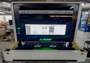
اختبار و إعداد نماذج أولية للطبقات المطبوعة عالية التردد
عندما تقوم بتطوير طبقات PCBs عالية التردد، تكون مراحل الاختبار وإعداد النماذج الأولية لا تقل أهمية عن باقي المراحل – فهي ضمان الجودة والموثوقية قبل الإنتاج بالكامل. تسمح لك هذه المراحل بالتحقق من المشاكل المحتملة وتحسين تصميمك، وضمان أن طبقات PCBs تتوافق مع معاييرك ومعايير الصناعة. دعونا نستكشف الاختبارات الأساسية وأساليب إعداد النماذج الأولية التي تُعتبر حاسمة لطبقات PCBs عالية التردد، وتوجيهك حول كيفية جعل هذه الخطوات ركنًا أساسيًا في عملية التصميم.
الاختبارات الأساسية لطبقات PCBs عالية التردد
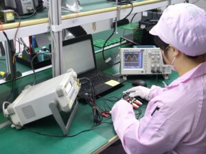
اختبار التأثير الزمني (TDR): هذا الاختبار ضروري لقياس خصائص.Impedance لطبقة PCB. يساعدك اختبار TDR على الكشف عن أي انقطاعات في الـImpedance التي يمكن أن تسبب انعكاسات الإشارة، مما هو حاسم لضمان السلامة الإشارة عند الترددات العالية.
اختبارات السلامة الإشارة: قم بإجراء اختبارات لتحليل جودة الإشارات على طبقة PCB. تشمل هذه الاختبارات قياس معاملات مثل زمن الصعود والهبوط، والتشويش، ومخططات العين، وضمان أن الإشارات قوية وواضحة خالية من التداخل، حتى عند الترددات العالية.
اختبار التوافق الكهرومغناطيسي (EMC): لضمان أن طبقة PCBs عالية التردد لا تنتج تداخلًا كهرومغناطيسيًا غير مرغوب فيه (EMI) أو أن تكون حساسة للتداخل الخارجي، فإن اختبار EMC هو أمر بالغ الأهمية. يساعدك هذا على التحقق من أن طبقة PCBs تتوافق مع معايير التوافق الكهرومغناطيسي الدولية، وهو ما يُعتبر حاسمًا للقبول في السوق.
اختبار الحرارة: منذ أن يمكن للعمليات عالية التردد أن تولد حرارة كبيرة، فإن إجراء اختبارات حرارية باستخدام كاميرات أو أجهزة استشعار حرارية يكون ضروريًا. هذا يضمن أن استراتيجيات إدارة الحرارة الخاصة بك تكون فعالة وأن طبقة PCBs يمكنها العمل بشكل موثوق عند ظروف درجة الحرارة المختلفة.
اختبار السلامة القدرة: تقييم أداء شبكة توزيع القدرة (PDN) على طبقة PCB لضمان أن tấtير المكونات تتلقى قدرة مستقرّة ونقيّة خالية من الضوضاء أو انخفاضات الجهد، وهو أمر حرج لتشغيل المكونات عالية التردد بشكل موثوق.
أهمية أساليب إعداد النماذج الأولية
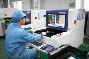
إعداد النماذج الأولية السريع: استخدم تقنيات مثل آلة CNC ل生产 نماذج أولية سريعة لطبقات PCB. هذا يسمح لك بالتكرار السريع للتصاميم بناءً على ملاحظات الاختبار، مما يزيد بشكل كبير من سرعة عملية التطوير.
طباعة طبقات PCB ثلاثية الأبعاد: لتصاميم معقدة أو غير تقليدية، يمكن استخدام الطباعة ثلاثية الأبعاد لطبقات PCB، مما يسمح بمرونة أكبر في التصميم والقدرة على اختبار أشكال يمكن أن تكون صعبة الإنتاج بالطرق التقليدية.
تصنيع منخفض الحجم: قبل الانتقال إلى الإنتاج بالكامل، يمكن أن يكون إنتاج كمية صغيرة من طبقات PCB قيمة große. يمكن استخدام هذه الدورة منخفضة الحجم لأداء اختبارات وظيفية شاملة وجمع ملاحظات من المستخدمين المحتملين أو الاختبارات الميدانية.
لماذا إعداد النماذج الأولية والاختبار مهمان
تقليل المخاطر: يقلل إعداد النماذج الأولية المبكر والمتكرر مع الاختبار الشديد من مخاطر الفشل في الإنتاج بالكامل. يساعد على تحديد عيوب التصميم وتصحيحها، وضمان أن المنتج النهائي ي مع المواصفات المطلوبة.
الكفاءة التكاليفية: تحديد المشاكل في مرحلة النموذج الأولي يكون أقل تكلفة من إجراء التغييرات خلال الإنتاج بالكامل أو، أسوأ من ذلك، استدعاء المنتجات المعيبة من السوق.
تحسين الأداء: يمنحك الاختبار وإعداد النماذج الأولية فرصة لتحسين أداء طبقات PCBs، وضمان أنها تعمل بفعالية قصوى ومُحسّنة للاستخدام المقصود.
ثقة أصحاب المصلحة: يبني عرض طبقات PCBs التي تم اختبارها وتحضير نماذج أولية لها بعمق ثقة بين أصحاب المصلحة، بمن فيهم المستثمرين والعملاء والهيئات التنظيمية، بأن المنتج موثوق به وجاهز للسوق.
من خلال دمج الاختبار الشامل وتحضير النماذج الأولية القوية في عملية التطوير، يمكنك ضمان أن طبقات PCBs عالية التردد لا تكون وظيفية فحسب، بل تكون آلات محسنة جيدًا لتلبيجات البيئات التقنية الكثيفة التي ستعمل فيها. تذكر، هذه الخطوات هي أدواتك الأفضل لتقليل المخاطر وتحسين منتجاتك قبل إطلاقها في السوق.

الفصل 9
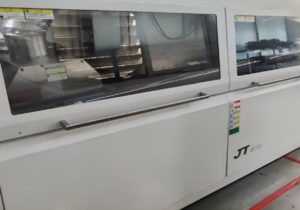
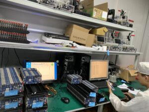
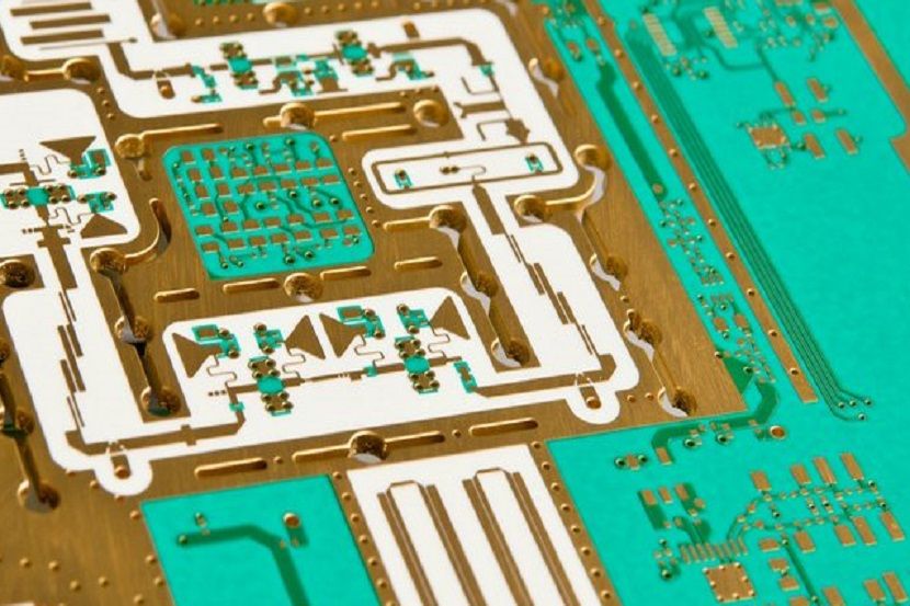
عمليات التصنيع للوحات الدائرة المطبوعة عالية التردد
عندما تغوص في تصنيع لوحات الدائرة المطبوعة عالية التردد، فأنت تدخل مجالاً حيث الدقة والالتزام بمعايير الجودة ليسا مجرد أهداف، بل هو ضروري. كل خطوة في عملية التصنيع تلعب دورًا حاسمًا في تحديد أداء وموثوقية المنتج النهائي. فهم دقة هذه العمليات وكيف تؤثر التقنيات المختلفة على النتيجة أمر بالغ الأهمية. في هذا المنشور، سنستكشف العالم المتقدم لتصنيع لوحات الدائرة المطبوعة عالية التردد، وإرشادك خلال كل خطوة وتأثيرها على اللوحة النهائية.
موجز لعملية التصنيع للوحات الدائرة المطبوعة عالية التردد
اختيار المواد: تبدأ الرحلة باختيار المواد المناسبة. بالنسبة للوحات الدائرة المطبوعة عالية التردد، تفضل المواد مثل PTFE و Rogers واللامينات المليئة بالسيراميك بسبب ثوابتها العازلة المنخفضة ومقادير الفقد، مما يسهم في تقليل فقد الإشارات وضمان سلامة الإشارات عند الترددات العالية.
طباعة نمط الدائرة: يتم نقل تصميم لوحة الدائرة المطبوعة عالية التردد إلى القاعدة المختارة باستخدام تقنيات طباعة متقدمة. يمكن أن يتضمن ذلك التصوير الضوئي، حيث يتم تطبيق مقاوم للضوء وتعريضه للضوء لإنشاء نمط الدائرة، أو تقنيات التصوير المباشر لتصاميم أكثر تعقيدًا أو دقة.
الحفر: بعد طباعة نمط الدائرة، يتم إزالة النحاس غير المرغوب فيه من خلال عملية حفر. الدقة في هذه الخطوة أمر حيوي؛ أي انحراف يمكن أن يؤثر على.Impedance وأداء الإشارات عالية التردد. يتم استخدام تقنيات حفر خاضعة للرقابة لضمان حل النحاس غير المرغوب فيه فقط، مع ترك نمط دائرة نظيف ودقيق.
تركيب الطبقات والتلايم: يتم تركيب طبقات متعددة من اللوحة وطبق التلايم تحت الحرارة والضغط. بالنسبة للوحات الدائرة المطبوعة عالية التردد، من المهم ضمان أن يتم تركيب كل طبقة بطريقة مثالية للحفاظ على سلامة المسارات الكهربائية وضبط.Impedance الفعال. أي انحراف يمكن أن يؤدي إلى مشاكل في سلامة الإشارات وتقليل الأداء.
الحفر والتطبيق: يتم حفر ثقوب أو مسارات لإنشاء اتصالات بين طبقات اللوحة المختلفة. لهذه التطبيقات عالية التردد، دقة وضع المسارات وحودة التطبيق داخلها أمر بالغ الأهمية. يجب أن تكون هذه المسارات موزعة بشكل مثالي وتملك تطبيقًا ناعمًا من النحاس لضمان اتصالات كهربائية موثوقة والحفاظ على سلامة الإشارات.
تطبيق غطاء اللحام: يتم تطبيق غطاء لحام على مسارات النحاس لحمايتها من الأكسدة ومنع جسور اللحام أثناء وضع المكونات. بالنسبة للوحات الدائرة المطبوعة عالية التردد، يجب تطبيق غطاء اللحام بشكل موحد لمنع أي مشاكل في السعة أو العزل غير مقصودة.
تجهيز السطح: تحصل اللوحة على تغطية سطح تعمل كتغطية حامية وتوفر سطحًا موثوقًا لل لحام لتركيب المكونات. يتم اختيار خيارات مثل ENIG (النيكل الكهربي الغير نشط والذهب المغمور) أو HASL (مستوى لحام الهواء الساخن) بناءً على تأثيرها على سلامة الإشارات ومتطلباتها للتطبيقات عالية التردد.
الاختبار ومراقبة الجودة: تخضع كل لوحة دائرة مطبوعة عالية التردد لاختبارات صارمة، بما في ذلك اختبار.Impedance واختبارات سلامة الإشارات واختبارات الوظيفة. هذه الاختبارات تضمن أن تلبي كل لوحة المتطلبات الصارمة اللازمة للعمليات عالية التردد.
تأثير تقنيات التصنيع المختلفة على المنتج النهائي
تدوير المواد المتقدمة: استخدام مواد متخصصة مثل PTFE يتطلب تعديلات في عمليات تصنيع اللوحة المطبوعة القياسية، مثل تقنيات الحفر والتلايم المعدلة لتعامل هذه المواد الحساسة دون إتلاف خصائصها.
الهندسة الدقيقة: متطلبات الدقة العالية في الحفر والتحويل وتركيب الطبقات تزداد في تصنيع لوحات الدائرة المطبوعة عالية التردد. الانحرافات الصغيرة يمكن أن تؤثر بشكل كبير على الأداء، مما يجعل الهندسة الدقيقة ركنًا أساسيًا من العملية.
تقنيات التغطية المتخصصة: يؤثراختيار غطاء السطح بشكل أكبر على لوحات الدائرة المطبوعة عالية التردد، حيث يمكن أن تؤدي بعض الأغلفة إلى إحداث سعة أو حث غير مرغوب فيها. اختيار الغطاء المناسب أمر بالغ الأهمية للحفاظ على أداء الإشارات المثالي.
من خلال إتقان هذه العمليات التصنيعية وفهم آثاره، تضمن أن لوحات الدائرة المطبوعة عالية التردد لا تعمل فقط كما هو مقصود، ولكنها también تقاوم متطلبات التطبيقات الإلكترونية الحديثة. كل خطوة، من اختيار المواد إلى الاختبار النهائي، تهدف إلى تحقيق أعلى جودة وأداء، مما يضمن أن لوحاتك تعمل بأفضل ما يمكن في ما يهم بشكل أكبر.
الفصل 10
اتجاهات المستقبل في تصميم بطاقات الدائرة المطبوعة عالية التردد
نظرًا لاتجاهنا نحو الأفق في تصميم بطاقات الدائرة المطبوعة عالية التردد، من الواضح أن المجال مستعد للتغييرات التحويلية. التكنولوجيا والmaterials الواعدة تحدد المشهد من أجل التطورات الثورية التي ستغير شكل كيفية تصميم واستخدام بطاقات الدائرة المطبوعة في تطبيقات التردد العالي. دعونا نستكشف ما تتضمنه هذه الاتجاهات وكيف قد تؤثر على مشهد تقنية بطاقات الدائرة المطبوعة في المستقبل.
التكنولوجيا والmaterials الواعدة
قواعد البوليمر البلوري السائل (LCP): يكتسب البوليمر البلوري السائل اهتمامًا كمادة قاعدة لبطاقات الدائرة المطبوعة عالية التردد بسبب خصائصه الكهربائية الممتازة، بما في ذلك ثوابت دييلكتريك وloss tangent منخفضة، والتي هي ضرورية لتقليل فقد الإشارات وتحقيق سلامة الإشارات القصوى. كما أن LCP مقاوم للرطوبة بشكل كبير وله استقرار حراري ممتاز، مما يجعله مثاليًا للبيئات القاسية.
الأجهزة السلبية المتكاملة (IPDs): يعتبر دمج المكونات السلبية مباشرة على قاعدة بطاقة الدائرة المطبوعة اتجاهًا متزايدًا. تساعد IPDs في تقليل حجم ووزن تجمعات بطاقة الدائرة المطبوعة وتعزيز سلامة الإشارات عن طريق تقليل الاتصالات وتحسين الموثوقية عن طريق تقليل عدد مفاصل اللحام. هذه التكنولوجيا مفيدة بشكل خاص في تطبيقات التردد العالي مثل الاتصالات وأبحاث الفضاء.
الإلكترونيات المطبوعة ثلاثية الأبعاد: من المتوقع أن تغير التصنيع الإضافي أو الطباعة ثلاثية الأبعاد صناعة بطاقات الدائرة المطبوعة من خلال السماح بهياكل أكثر تعقيدًا وهياكل متعددة الأبعاد. تمكن هذه التكنولوجيا من دمج الوظائف الإلكترونية في نسيج المكونات نفسه، ما يفتح طرقًا جديدة لتقليل حجم الأجهزة وتطبيقات التردد العالي المعقدة.
بطاقات الدائرة المطبوعة المرنة والقابلة للتمديد: مع زيادة الطلب على تقنيات Wearable والإلكترونيات المرنة، يزداد الحاجة إلى بطاقات الدائرة المطبوعة التي يمكن أن تتكيف وتتمدد. يتم تطوير مواد وتقنيات تصنيع جديدة لإنتاج بطاقات الدائرة المطبوعة المرنة عالية التردد التي يمكنها الحفاظ على الأداء تحت التوتر والتشوه الميكانيكي.
تنبؤات حول كيفية تأثير هذه التطورات على الشكل المستقبلية
التكامل والتصغير الأكبر: من المحتمل أن نشهد مستقبلًا لبطاقات الدائرة المطبوعة عالية التردد بأحجام وأشكال أكثر جمعًا وتكاملًا. ستمكن التكنولوجيا مثل IPDs والطباعة ثلاثية الأبعاد المصممين من دمج المزيد من الوظائف في مساحات أصغر، ما يدفع حدود التصغير مع تحسين الأداء والموثوقية.
أداء محسن في البيئات القاسية: مع مواد مثل LCP، ستكون بطاقات الدائرة المطبوعة عالية التردد المستقبلية أكثر متانة وقدرة على العمل في ظل ظروف بيئية قاسية. سيكون هذا حاسمًا لتوسيع استخدام الإلكترونيات عالية التردد في قطاعات مثل الطيران والصناعات العسكرية والسيارات.
اعتماد أوسع لبطاقات الدائرة المطبوعة المرنة والقابلة للتمديد: سيؤدي استمرار تطوير القواعد المرنة إلى انتشار أوسع في الإلكترونيات الاستهلاكية والأجهزة الطبية وحتى في مجالات جديدة مثل الروبوتات الناعمة. لن تكون هذه البطاقات بحاجة فقط إلى الأداء في الترددات العالية ولكن أيضًا إلى تحمل الانحناء والتمديد، ما يreamble المصممين إلى التفكير خارج النماذج التقليدية.
الاستدامة في تصنيع بطاقات الدائرة المطبوعة: مع تزايد القلق البيئي، من المحتمل أن تتجهصناعة بطاقات الدائرة المطبوعة نحو عمليات تصنيع أكثر استدامة. قد يشمل هذا استخدام مواد بيولوجية، قواعد قابلة لإعادة التدوير، وتقنيات تصنيع كفية في استهلاك الطاقة.
أدوات اختبار ومحاكاة متقدمة: مع زيادة تعقيد بطاقات الدائرة المطبوعة عالية التردد، ستصبح أدوات المحاكاة والاختبار المتقدمة أكثر أهمية. ستحتاج هذه الأدوات إلى التنبؤ والتقليل من المشاكل المرتبطة بال تداخل الكهرومغناطيسي، وإدارة الحرارة، والتوتر الميكانيكي قبل بناء النماذج المادية.
من خلال البقاء في طليعة هذه الاتجاهات، لن تكون فقط مستعدًا لمستقبل تصميم بطاقات الدائرة المطبوعة عالية التردد بل تشكله أيضًا. كل تقدم يbringنا أقرب إلى أجهزة إلكترونية أكثر قوة وفعالية وتنوعًا، مما يفتح عصرًا جديدًا من التكنولوجيا يتجاوز حدود اليوم.
تواصل معنا
أين نحن؟
الحديقة الصناعية، رقم 438 شارع دونغ هوان، رقم 438، شاجينغ دونغ هوان، منطقة باوان، شنتشن، قوانغدونغ، الصين
الطابق 4، مبنى زهيهوي الإبداعي، رقم 2005 شارع شيهوان، شاجينغ، منطقة باوان، شنتشن، الصين
الغرفة A1-13، الطابق 3، مركز يي ليم الصناعي، 2-28 شارع كواي لوك، كواي تشونغ، هونغ كونغ
service@southelectronicpcb.com
الهاتف: +86 400 878 3488
أرسل لنا رسالة

Need a reliable PCB/PCBA partner?
Fast quote, stable quality, and turnkey support for your projects.
Industries
WhatsApp us
Send Us a Message
The more detailed you fill out, the faster we can move to the next step.
