
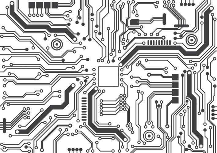
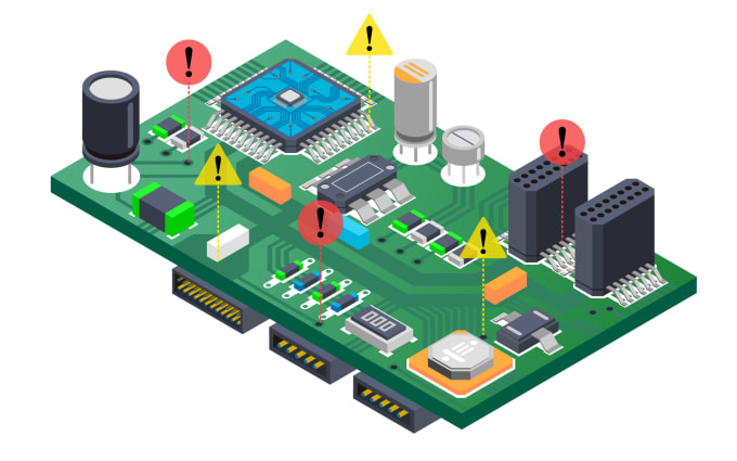
تصميم لوحات الدوائر المطبوعة متعددة الطبقات
South-Electronic
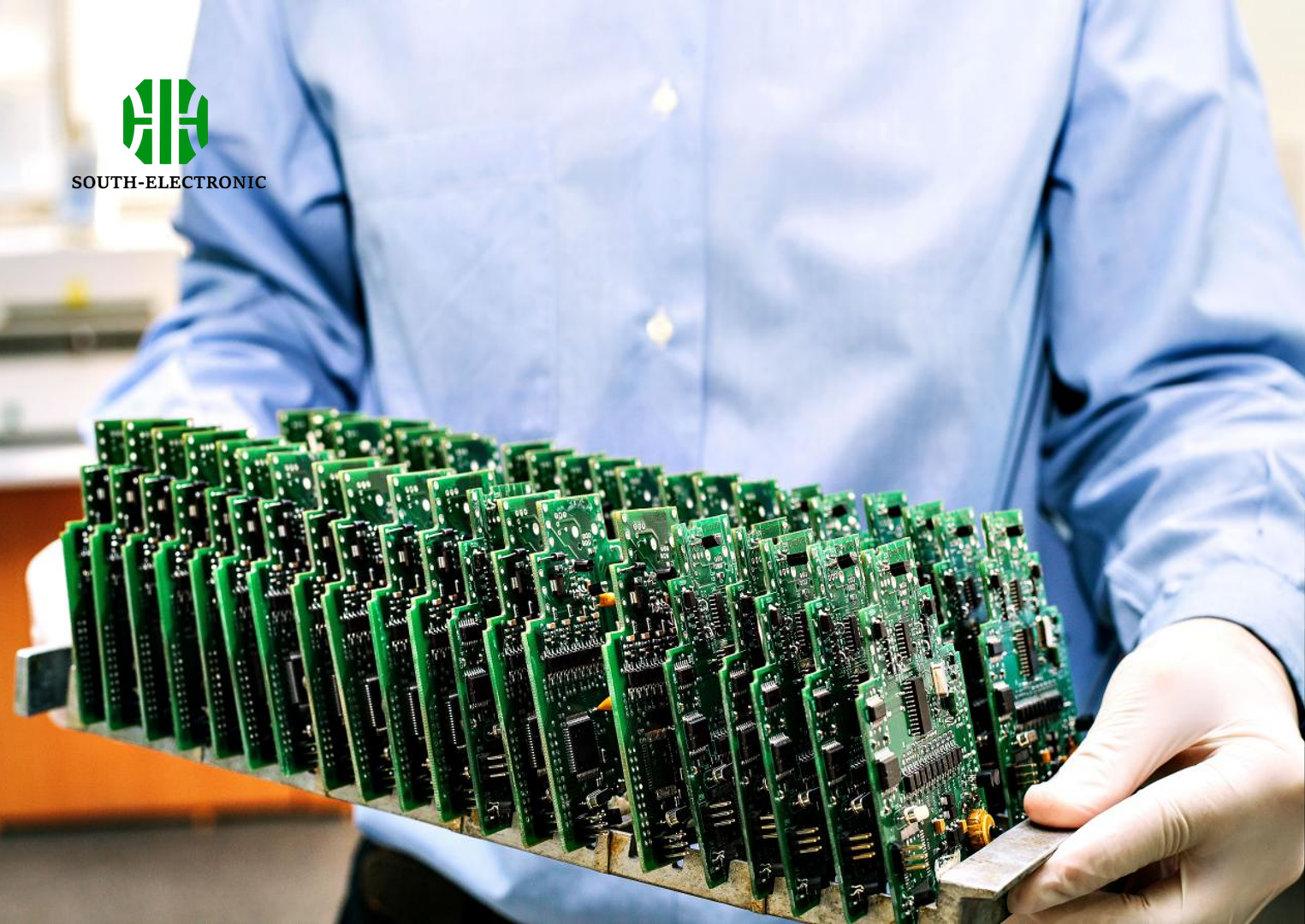
تقدم خدمة South-Electronic الشاملة مشروعك بسلاسة من المفهوم إلى الواقع، مع ضمان الأداء العالي والمتانة في كل مرحلة. مع أكثر من عقد من الخبرة، يقدم فريقنا الخبير حلولًا مخصصة لتلبية أكثر المتطلبات تعقيدًا، وكل ذلك بأسعار تنافسية. استمتع بالتسليم السريع، الدعم على مدار الساعة، وخدمة ما بعد البيع مدى الحياة. ثق بـ South-Electronic لرفع أجهزتك الإلكترونية إلى مستويات جديدة من النجاح!
لماذا تختار South-Electronic؟
يمكنك الوثوق بـ South-Electronic لتقديم جودة لا مثيل لها، وموثوقية، وقيمة استثنائية.
مع خدمة تصميم لوحات الدوائر المطبوعة متعددة الطبقات الشاملة لدينا، ستستمتع برحلة سلسة من المفهوم إلى الإنجاز. نحن نضمن الدقة، والمتانة، والالتزام الصارم بمعايير الصناعة، لضمان رضاك في كل خطوة.
-
تصميم مخصص
تصميم مخصص لتلبية احتياجاتك الفريدة.
في South-Electronic، ندرك أن كل مشروع فريد من نوعه. لذلك، نقدم خدمات تصميم لوحات الدوائر المطبوعة (PCB) المخصصة لتلبية متطلباتك المحددة، مما يضمن تنفيذ كل تفصيلة بدقة وفقًا لمواصفاتك. هذا يعزز أداء وموثوقية منتجاتك. -
ضمان الرضا
ستقدر الثقة التي تأتي من العمل مع شركة معتمدة بشهادة ISO9001.
نحن نعطي الأولوية للاتصال الواضح والشفاف ونلتزم بأعلى المعايير، لضمان أن لوحات الدوائر المطبوعة متعددة الطبقات الخاصة بك لا تقتصر فقط على تلبية توقعاتك، بل تتجاوزها من حيث الأداء، والمتانة، والدقة. -
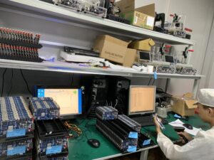
خدمة شاملة
تحصل على رضا تام مع مجموعة واسعة من المعدات لدينا.
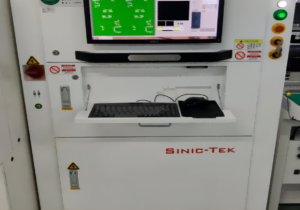
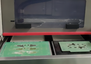
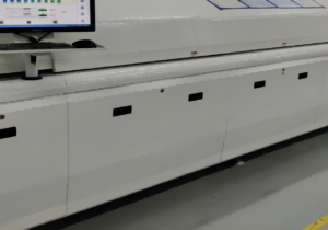
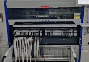
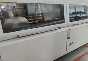
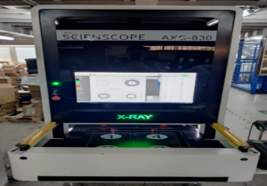
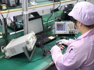
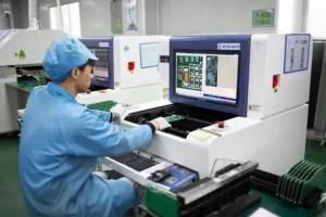
لدينا مجموعة واسعة من قدرات معالجة لوحات الدوائر المطبوعة. من التصميم إلى التسليم، لدينا المعدات والعمليات اللازمة لضمان إنجاز طلبك بشكل صحيح. -
تسليم سريع
ابقَ على الموعد المحدد مع أوقات التنفيذ السريعة لدينا.
تضمن عمليات الإنتاج المبسطة لدينا أوقات تسليم سريعة، بحيث تحصل على منتجاتك في الوقت الذي تحتاجها، دون أي تأخير.
المشاريع ذات الصلة التي قمنا بها
آراء العملاء
الأسئلة الشائعة
أكثر الأسئلة شيوعًا
Send us a message
The more detailed you fill out, the faster we can move to the next step.


الدليل الشامل لتصميم لوحات الدوائر المطبوعة متعددة الطبقات
الفهرس
الفصل 1

مقدمة إلى لوحات الدوائر المطبوعة متعددة الطبقات
ما هي لوحات الدوائر المطبوعة متعددة الطبقات ولماذا هي مهمة؟
لوحة الدوائر المطبوعة متعددة الطبقات (Multilayer PCB) هي نوع معقد من لوحات الدوائر يتكون من عدة طبقات من المكونات الكهربائية مفصولة بطبقات عازلة. على عكس لوحات الدوائر أحادية الطبقة التقليدية، التي تحتوي على مكونات على جانب واحد فقط من اللوحة، تتكدس لوحات الدوائر متعددة الطبقات عدة طبقات فوق بعضها البعض، مع فصل كل طبقة بطبقة عازلة. يسمح هذا التصميم بتجميع المزيد من المكونات في مساحة أصغر، مما يزيد من كفاءة وأداء الجهاز.
الانتقال من لوحات الدوائر أحادية الطبقة إلى متعددة الطبقات
يمثل الانتقال من لوحات الدوائر أحادية الطبقة إلى متعددة الطبقات تقدمًا كبيرًا في تكنولوجيا تصميم الإلكترونيات. في بدايات الإلكترونيات، كانت لوحات الدوائر أحادية الطبقة كافية لتلبية احتياجات الأجهزة الإلكترونية الأولى. ومع ذلك، مع تقدم التكنولوجيا، زاد الطلب على أجهزة أصغر وأسرع. أدى ذلك إلى تطوير لوحات الدوائر ثنائية الطبقة، وأخيرًا، متعددة الطبقات.
تسمح كل طبقة إضافية بكثافة أعلى من المكونات والتوصيلات التي لا يمكن تحقيقها باستخدام التصاميم أحادية الطبقة. هذا الانتقال مكّن من إنشاء إلكترونيات أكثر تعقيدًا وقوة.
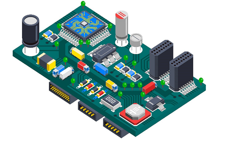
نظرة عامة على المكونات والوظائف
المكونات الرئيسية للوحات الدوائر المطبوعة متعددة الطبقات تشمل:
المسارات الموصلة (Traces):
خطوط نحاسية أو من مواد موصلة أخرى محفورة على اللوحة وتعمل كأسلاك الدائرة.الطبقات العازلة (Dielectric Layers):
طبقات عازلة تفصل الطبقات النحاسية الموصلة وتمنع حدوث قصر كهربائي بين الطبقات المختلفة.الثقوب (Vias):
ثقوب صغيرة تُحفر في اللوحة لتسمح بالتوصيلات الكهربائية بين الطبقات المختلفة. يمكن أن تكون الثقوب كاملة الاختراق، عمياء، أو مدفونة، اعتمادًا على الطبقات التي تربطها.الوسادات (Pads):
مناطق معدنية مكشوفة تُلحم عليها المكونات.
من حيث الوظائف، توفر لوحات الدوائر المطبوعة متعددة الطبقات العديد من المزايا مقارنة بألواح أحادية الطبقة:
سعة وكثافة أعلى:
يمكنها دعم مزيد من الدوائر لكل وحدة مساحة، وهو أمر ضروري للأجهزة الحديثة المدمجة.تحسين المتانة:
يوفر التصميم متعدد الطبقات حماية أكبر ضد العوامل البيئية مثل الحرارة والرطوبة.أداء معزز:
يمكن ترتيب الطبقات المتعددة لتقليل التداخل الكهرومغناطيسي (EMI) والخسائر الإشارية، وهو أمر حاسم للحفاظ على سلامة الإشارات عالية السرعة.
لقد غيّرت لوحات الدوائر المطبوعة متعددة الطبقات طريقة تصميمنا للإلكترونيات من خلال السماح لنا بمواكبة التكنولوجيا مع تقليل الحجم. تتيح هذه اللوحات وضع دوائر معقدة في مساحة صغيرة، وتجعل الأجهزة تعمل بشكل أفضل وتدوم لفترة أطول. ولهذا السبب تراها في كل شيء هذه الأيام.
الفصل 2
لماذا يجب عليك استخدام لوحات الدوائر المطبوعة متعددة الطبقات
وظائف أكثر في مساحة أصغر
إحدى أكبر مزايا لوحات الدوائر المطبوعة متعددة الطبقات هي أنها تتيح لك دمج وظائف أكثر في مساحة أصغر. وهذا أمر بالغ الأهمية في الصناعات التي تكون فيها المساحة محدودة. من خلال تكديس الطبقات المتعددة، تتيح هذه اللوحات توفير مساحة أكبر للمكونات والتوصيلات. وهذا يعني أنه يمكنك دمج وظائف أكثر في أجهزة أصغر، مثل الهواتف الذكية، الساعات الذكية، وزرعات الطبية، حيث لا تكون لوحات الدوائر أحادية الطبقة التقليدية كافية.
متانة وموثوقية أفضل
عندما تختار لوحات الدوائر المطبوعة متعددة الطبقات، فإنك تحصل على منتج أكثر متانة. تحتوي هذه اللوحات على عدة طبقات من المواد تشمل عوازل عالية الجودة تحمي الطبقات النحاسية الموصلة. لا يقتصر هذا الهيكل على الحماية من التهديدات البيئية مثل الرطوبة والإجهاد الحراري فحسب، بل يوفر أيضًا استقرارًا ميكانيكيًا. والنتيجة هي منتج يتحمل الظروف الصعبة لفترة أطول، مما يجعل لوحات الدوائر متعددة الطبقات مثالية للتطبيقات في البيئات القاسية، مثل الإلكترونيات السيارات، المعدات العسكرية، ومعدات الاتصالات الخارجية.
أداء أفضل مع تقليل التداخل الكهرومغناطيسي (EMI)
مع لوحات الدوائر المطبوعة متعددة الطبقات، يمكنك الحصول على أداء أفضل، خصوصًا فيما يتعلق بسلامة الإشارات. تم تصميم هذه اللوحات لتشمل طبقات داخلية للطاقة والأرضية تحجب الطبقات التي تحمل الإشارات، مما يقلل بشكل كبير من التداخل الكهرومغناطيسي (EMI). وهذا يجعلها مثالية للدوائر عالية السرعة حيث تكون سلامة الإشارة أمرًا بالغ الأهمية. يمكنك ملاحظة هذا التحسين في التطبيقات مثل مراكز البيانات، أجهزة التوجيه عالية السرعة، وأنظمة الحوسبة المتقدمة حيث يمكن أن يؤدي حتى القليل من التداخل إلى أخطاء في البيانات.
أساسية للأجهزة الحديثة المدمجة وعالية الكثافة
تعد فوائد لوحات الدوائر المطبوعة متعددة الطبقات أمرًا بالغ الأهمية في الإلكترونيات الحديثة التي من المتوقع أن تؤدي وظائف متعددة بينما تناسب مساحات أصغر بشكل متزايد. فكر في هاتفك الذكي الأخير أو طائرة بدون طيار متطورة—تتطلب هذه الأجهزة تكوينات مكونات كثيفة لا يمكن دعمها بكفاءة إلا من خلال لوحات الدوائر متعددة الطبقات. علاوة على ذلك، يوفر التصميم المرن لهذه اللوحات إمكانية وضع المكونات بشكل مثالي، مما يؤدي إلى تحسين الاتصال ومسارات نقل أقصر، وبالتالي تحسين الأداء العام للجهاز.
تُستخدم في مجموعة واسعة من الصناعات
تُستخدم لوحات الدوائر المطبوعة متعددة الطبقات في مجموعة واسعة من الصناعات، بما في ذلك الرعاية الصحية، الإلكترونيات الاستهلاكية، السيارات، والفضاء. في كل من هذه المجالات، يوفر الحجم الصغير، المتانة، والأداء لهذه اللوحات التقنية المطلوبة لدفع الابتكار. سواء كانت تقنية قابلة للارتداء تراقب صحتك، سيارات ذكية صديقة للبيئة، أو إلكترونيات الطيران، فإن لوحات الدوائر المطبوعة متعددة الطبقات هي المحرك الأساسي للتطورات التي توسع حدود ما يمكن للتكنولوجيا تحقيقه.
عندما تستخدم لوحات الدوائر المطبوعة متعددة الطبقات في تصاميمك، فإنك لا تواكب الاتجاهات الحالية في التكنولوجيا فحسب؛ بل تضع الأساس للابتكارات المستقبلية. بفضل جميع مزاياها، لا تلبي هذه اللوحات المعايير العالية اليوم فقط بل تتوقع أيضًا تحديات الغد، مما يجعلها جزءًا أساسيًا من تطور الأجهزة الإلكترونية.
الفصل 3
الاعتبارات الأساسية لتصميم لوحات الدوائر المطبوعة متعددة الطبقات
تصميم لوحة دوائر مطبوعة متعددة الطبقات أكثر تعقيدًا بكثير من تصميم لوحة أحادية الطبقة. إليك بعض الأمور التي تحتاج إلى التفكير فيها للتأكد من أن لوحة الدوائر المطبوعة متعددة الطبقات تعمل بشكل صحيح وتكون موثوقة.
اختيار المادة المناسبة
اختيار المادة المناسبة أمر بالغ الأهمية عند تصميم لوحة دوائر مطبوعة متعددة الطبقات. تؤثر المادة على كل شيء، بدءًا من متانة اللوحة وحتى كفاءتها في توصيل الكهرباء. المادة الأكثر شيوعًا هي FR-4، وهي عبارة عن مزيج من الألياف الزجاجية وراتنج الإيبوكسي. تُستخدم FR-4 على نطاق واسع لأنها تحقق توازنًا جيدًا بين التكلفة والأداء. إذا كنت تعمل على تطبيق عالي التردد، فقد تحتاج إلى استخدام مواد أكثر تقدمًا مثل Rogers أو Teflon التي تقلل الفاقد العازل.
تؤثر المادة التي تختارها على قدرة اللوحة على تحمل الحرارة، قوتها، وكفاءتها في توصيل الكهرباء. على سبيل المثال، المواد ذات معامل تمدد حراري منخفض (CTE) أفضل في إدارة الحرارة وأقل عرضة للمشاكل الميكانيكية عند تغير درجة الحرارة. هذا مهم بشكل خاص في الأجهزة ذات الكثافة العالية أو القدرة العالية حيث تكون الحرارة مشكلة كبيرة.
تحديد عدد الطبقات المطلوبة
تحديد عدد طبقات اللوحة أمر بالغ الأهمية لأنه يؤثر على تكلفة اللوحة وما يمكنها فعله. المزيد من الطبقات يسمح بإضافة مكونات أكثر وإنشاء دوائر أكثر تعقيدًا، وهو أمر مهم للإلكترونيات عالية الأداء. لكن كل طبقة إضافية تجعل اللوحة أكثر تكلفة وصعوبة في التصنيع.
عند تحديد عدد الطبقات، فكر في أهمية الحفاظ على إشارات سليمة واحتياجات اللوحة من الطاقة. إذا كنت تعمل على شيء يحتوي على إشارات سريعة جدًا، فقد تحتاج إلى طبقات مخصصة للطاقة والأرضية للتأكد من عمل كل شيء بشكل صحيح ومنع تداخل الإشارات.
عرض الخطوط: ضمان سلامة الإشارة وتحمل الطاقة
عرض الخطوط على اللوحة مهم جدًا لأنه يؤثر على مقدار التيار الذي يمكن أن تتحمله اللوحة دون أن تسخن، وكذلك على جودة الإشارات. الخطوط الرفيعة تتيح لك وضع المزيد من المكونات في مساحة أصغر، لكنها قد لا تتحمل تيارًا عاليًا، مما قد يؤدي إلى تسخينها أو حتى تلفها.
كما أن عرض الخطوط يلعب دورًا مهمًا في ضبط المقاومة الكهربائية (Impedance)، خصوصًا عند التعامل مع إشارات عالية السرعة. تحتاج إلى التأكد من ضبط المقاومة بشكل صحيح حتى لا ترتد الإشارات وتسبب مشاكل. توجد أدوات برمجية يمكنها مساعدتك في حساب عرض الخطوط المناسب بناءً على مقدار التيار والمقاومة المطلوبة لمشروعك.
معالجة التداخل الكهرومغناطيسي (EMI) والتداخل بين الإشارات (Crosstalk)
عند تصميم لوحة دوائر مطبوعة متعددة الطبقات، من المهم التفكير في كيفية منع التداخل بين الإشارات ومنع الضوضاء من التأثير عليها. إحدى الطرق هي وضع طبقات الطاقة والأرضية في أماكن مناسبة داخل اللوحة. يمكن أن يساعد ذلك في تقليل الضوضاء. كما يجب التفكير في كيفية تخطيط مسارات الإشارات. أحد الحلول هو استخدام الإشارات التفاضلية (Differential Signaling) التي تقلل من تأثير الضوضاء على الإشارات. كما يجب الحفاظ على مسافة كافية بين الخطوط لتجنب التداخل بينها.
تصميم الثقوب (Vias): توصيل الطبقات بشكل فعال
الثقوب (Vias) هي جزء مهم جدًا في تصميم اللوحات متعددة الطبقات. يجب أن تقرر ما إذا كنت ستستخدم ثقوبًا كاملة (Through-hole)، ثقوبًا عمياء (Blind Vias)، أو ثقوبًا مدفونة (Buried Vias)، بناءً على احتياجات مشروعك وميزانيتك. الثقوب الكاملة هي الأرخص والأسهل في التصنيع، لكنها تشغل مساحة كبيرة. أما الثقوب العمياء والمدفونة فتسمح بتوفير المساحة وتحسين أداء اللوحة، لكنها تزيد من تعقيد وكلفة التصنيع.
إذا أخذت هذه العوامل في الاعتبار—اختيار المواد، عدد الطبقات، عرض الخطوط، منع التداخل، ونوع الثقوب—يمكنك تصميم لوحة دوائر مطبوعة متعددة الطبقات تعمل بكفاءة وبتكلفة معقولة. هذه القرارات لا تؤثر فقط على كيفية عمل اللوحة، بل تؤثر أيضًا على التكلفة وسهولة التصنيع. عند العمل على تصميم لوحة جديدة، فكر في هذه الأمور للتأكد من أنك تصمم لوحة جيدة وسهلة الإنتاج.
الفصل 4
عملية تصميم لوحات الدوائر المطبوعة متعددة الطبقات خطوة بخطوة
تصميم لوحة دوائر مطبوعة متعددة الطبقات هو نشاط منهجي يحتاج إلى التنفيذ بعناية. سواء كنت مصممًا محترفًا للوحات الدوائر المطبوعة أو بدأت رحلتك للتو، فإن اتباع نهج منظم سيضمن وظيفة وموثوقية منتجك النهائي. اتبع هذه الخطوات وستنجح في تصميم أول لوحة دوائر مطبوعة متعددة الطبقات.
الخطوة 1: الفكرة وتحليل المتطلبات
قبل أن تبدأ في تصميم لوحتك، يجب أن تكون واضحًا بشأن ما تريد تحقيقه وما الذي تحتاج اللوحة للقيام به. ما هو الغرض من اللوحة؟ ما هي الظروف البيئية التي ستتعرض لها؟ معرفة إجابات هذه الأسئلة سيساعدك في اختيار المواد المناسبة، والمكونات التي ستستخدمها، وعدد الطبقات والاتصالات التي ستحتاجها. قم بإعداد قائمة بجميع المكونات التي تخطط لاستخدامها واجمع أوراق البيانات الخاصة بها للرجوع إليها.
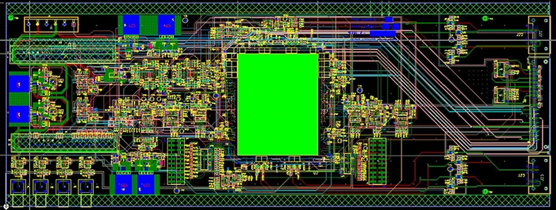
الخطوة 2: تصميم المخطط الكهربائي (Schematic)
باستخدام أداة تصميم PCB، ابدأ بإنشاء المخطط الكهربائي لدائرتك. يشمل ذلك رسم مخطط يُظهر جميع المكونات وكيفية اتصالها. من المهم جدًا التحقق من كل اتصال بدقة في هذه المرحلة لأن الأخطاء هنا يمكن أن تسبب مشاكل كبيرة لاحقًا. يمكن استخدام أدوات مثل OrCAD أو Altium Designer أو Eagle لتصميم المخطط. توفر هذه الأدوات تمثيلًا مرئيًا يساعدك في التأكد من أن كل شيء في مكانه الصحيح ويعمل كما يجب.
الخطوة 3: تخطيط تكوين الطبقات (Layer Stackup)
بعد الانتهاء من المخطط، تحتاج إلى تخطيط تكوين الطبقات. يشمل ذلك تحديد عدد الطبقات التي ستحتويها اللوحة وما دور كل طبقة. التكوينات الشائعة تشمل طبقات الإشارة، ومستويات الطاقة، ومستويات الأرضي. الهدف هو تقليل مشاكل سلامة الإشارة وإدارة التداخل الكهرومغناطيسي (EMI). بالنسبة للدوائر عالية السرعة، ضع في اعتبارك وضع طبقات الأرضي بجانب طبقات الإشارة لتوفير الحماية والتحكم في المقاومة.
الخطوة 4: تصميم التخطيط (Layout Design)
انتقل من المخطط الكهربائي إلى تصميم التخطيط في برنامج تصميم اللوحات. في هذه المرحلة، ستقوم بوضع المكونات وتوجيه المسارات بينها بناءً على الاتصالات التي حددتها في المخطط. انتبه جيدًا لوضع المكونات الحرجة لتقليل طول المسارات، مما يقلل التأخير والتداخل. استخدم أدوات التوجيه التلقائي مع التعديلات اليدوية لتحسين مسارات التوصيل والتأكد من أن المسارات عريضة بما يكفي لتحمل التيار وتلبية متطلبات المقاومة.
الخطوة 5: التحقق وفحص سلامة الإشارة
بعد الانتهاء من التخطيط، تحتاج إلى التأكد من أن كل شيء يلبي المتطلبات. استخدم الأدوات المتوفرة في برنامج تصميم اللوحات للتحقق من الأخطاء مثل تقاطع المسارات، عدم وجود مساحة كافية بين المسارات والمكونات، والمشاكل الأخرى المحتملة. قم بإجراء تحليل لسلامة الإشارة للتأكد من أن جميع الإشارات سيتم نقلها مع أدنى فقد وتداخل. قد تتطلب هذه الخطوة عدة تعديلات لتحسين التخطيط للحصول على أفضل أداء.
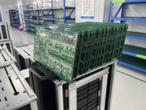
الخطوة 6: تصنيع النموذج الأولي
بمجرد التحقق من تصميمك، تكون جاهزًا لتصنيع نموذج أولي. سيتيح لك ذلك اختبار اللوحة في ظروف حقيقية واكتشاف أي مشاكل في الأداء أو الوظيفة. اختر مصنعًا موثوقًا للوحات الدوائر المطبوعة وقدم لهم ملفات التصميم الخاصة بك، عادةً بصيغة Gerber التي تحتوي على جميع البيانات اللازمة لتصنيع اللوحة.
الخطوة 7: الاختبار والتكرار
اختبر النموذج الأولي في ظروف مشابهة للظروف التي سيتم استخدامها فيها. تحقق من الوظيفة وأي اختلافات في الأداء. إذا وجدت أي مشاكل، عد إلى التصميم وقم بإجراء التعديلات اللازمة. قد يعني ذلك العودة إلى أي من الخطوات السابقة، بدءًا من تغيير المخطط إلى تغيير التخطيط أو حتى تغيير تكوين الطبقات.
الخطوة 8: الإنتاج النهائي
بعد اختبار النموذج الأولي وإجراء التعديلات اللازمة، يصبح تصميم اللوحة جاهزًا للإنتاج. يعني ذلك تكثيف عملية التصنيع لإنتاج العدد المطلوب من اللوحات، والتأكد من أن كل دفعة تُصنع بنفس معايير الجودة للنموذج الأولي.
إذا اتبعت هذه الخطوات بعناية، ستتمكن من تصميم وتصنيع لوحة دوائر مطبوعة متعددة الطبقات بجودة عالية تؤدي وظيفتها وتعمل بشكل موثوق في العالم الحقيقي. كل خطوة مهمة وتتطلب تفكيرًا دقيقًا للتأكد من نجاح منتجك الإلكتروني.
الفصل 5
استراتيجيات لإنشاء تكديس طبقات فعال للوحات الدوائر المطبوعة متعددة الطبقات
عند تصميم تكديس الطبقات للوحات الدوائر المطبوعة متعددة الطبقات، فإنه يشبه وضع أساس متين لمبنى. يعد هذا أمرًا بالغ الأهمية لاستقرار اللوحة ووظائفها وسلامتها. في هذا الفصل، سنستعرض الاستراتيجيات لإنشاء تكديس طبقات فعال، مع التركيز على تحسين كل من سلامة الإشارة والطاقة.
فهم تكديس الطبقات
تكديس الطبقات يشير إلى كيفية ترتيب الطبقات المختلفة (الإشارة، الطاقة، والأرضي) في لوحة الدوائر المطبوعة متعددة الطبقات. يؤثر هذا الترتيب على الأداء الكهربائي للوحة، بالإضافة إلى إمكانية تصنيعها وتكلفتها. يساعد التكديس الأمثل في تقليل مشاكل سلامة الإشارة، وإدارة التداخل الكهرومغناطيسي (EMI)، وضمان توزيع طاقة قوي.
الاستراتيجية 1: التركيز على سلامة الإشارة
للحفاظ على سلامة الإشارة، يجب أن يقلل التكديس من المسافة التي تقطعها الإشارات بين المكونات، مما يقلل من فرص فقدان الإشارة والتداخل. إليك كيفية القيام بذلك:
تزاوج الطبقات المتجاورة:
ضع طبقات الإشارة بجانب طبقات الأرضي أو الطاقة. سيوفر هذا حماية لطبقات الإشارة ومسار عودة للإشارة، مما يقلل التداخل الكهرومغناطيسي (EMI).التماثل والتوازن:
حاول الحفاظ على التكديس متماثلًا لمنع انحراف اللوحة أثناء التصنيع. التكديس المتماثل يضمن أيضًا خصائص كهربائية متسقة للوحة.
الاستراتيجية 2: تحسين سلامة الطاقة
تتمحور سلامة الطاقة حول الحفاظ على توزيع طاقة مستقر ونظيف عبر اللوحة. لتحقيق ذلك، يجب وضع طبقات الطاقة والأرضي بشكل استراتيجي:
استخدام طبقات مخصصة للطاقة والأرضي:
استخدم طبقات مخصصة للطاقة والأرضي. سيؤدي ذلك إلى تقليل مقاومة شبكة توزيع الطاقة وتوزيع الحمل الكهربائي بفعالية، وهو أمر بالغ الأهمية للتطبيقات عالية الطاقة.تقريب طبقات الطاقة والأرضي:
عند وضع طبقات الطاقة والأرضي بالقرب من بعضها البعض، يمكنك تقليل الحث الكلي للشبكة.
الاستراتيجية 3: تقليل التداخل الكهرومغناطيسي (EMI) والمشاكل الحرارية
يمكن أن يساعد التكديس الفعال أيضًا في تقليل التداخل الكهرومغناطيسي (EMI) وإدارة الأداء الحراري:
تناوب طبقات الأرضي:
استخدم طبقات أرضي متعددة متداخلة بين طبقات الإشارة. يعمل هذا الإعداد كدرع ضد EMI ويساعد في تبديد الحرارة، وهو أمر مهم بشكل خاص في التطبيقات عالية السرعة أو التردد.الثقوب الحرارية (Thermal Vias):
قم بتضمين ثقوب حرارية في التكديس لنقل الحرارة من المكونات الساخنة إلى المشتت الحراري أو البيئة الخارجية، مما يمنع ارتفاع درجة الحرارة.
الاستراتيجية 4: مراعاة تقنيات الاتصال عالي الكثافة (HDI)
بالنسبة للتصاميم المعقدة أو المدمجة للغاية، قد ترغب في استخدام تقنيات الاتصال عالي الكثافة (HDI). تتميز لوحات HDI بفواصل وخطوط دقيقة، وثقوب أصغر، وكثافة توصيل أعلى مقارنة بلوحات الدوائر التقليدية:
الثقوب الدقيقة (Microvias):
استخدم الثقوب الدقيقة لتوصيل الطبقات التي تحتاج إلى الاتصال فقط، مما يوفر المساحة ويحسن سلامة الإشارات عالية السرعة.الثقوب المكدسة (Stacked Vias):
استخدم الثقوب المكدسة في المناطق ذات الكثافة العالية للمكونات لتعظيم المساحة وتحسين الاتصال بين الطبقات.
إتمام التكديس
بعد التخطيط لتكديس الطبقات باستخدام هذه الاستراتيجيات، قم بمراجعته مع مصنع لوحات الدوائر المطبوعة الخاص بك. يمكنهم تقديم ملاحظات قيمة، خاصة فيما يتعلق بإمكانية التصنيع وتكاليفها. يمكنهم أيضًا تقديم رؤى حول أحدث المواد والتقنيات التي يمكن أن تحسن تصميمك بشكل أكبر.
تذكر أن تكديس الطبقات الذي تختاره يؤثر بشكل مباشر على أداء وموثوقية لوحة الدوائر المطبوعة متعددة الطبقات. من خلال التخطيط بعناية لاستراتيجية التكديس، تضمن أن لوحتك تلبي جميع المعايير الكهربائية الضرورية وتؤدي وظيفتها بشكل موثوق في تطبيقها المقصود.
الفصل 6
سلامة الإشارة والتحكم في المقاومة في لوحات الدوائر المطبوعة متعددة الطبقات
تُعتبر سلامة الإشارة والتحكم في المقاومة من أهم جوانب تصميم لوحات الدوائر المطبوعة متعددة الطبقات، خاصة عند التعامل مع الدوائر الإلكترونية عالية السرعة. في هذا الفصل، سنوضح أهمية هذين العنصرين وكيفية التعامل معهما بشكل فعال لضمان تحقيق الأداء الأمثل للوحة الدوائر المطبوعة الخاصة بك.
ما هي سلامة الإشارة؟
تشير سلامة الإشارة إلى الحالة التي يتم فيها نقل الإشارات الرقمية والتناظرية دون تدهور كبير. في لوحات الدوائر المطبوعة متعددة الطبقات، الحفاظ على سلامة الإشارة أمر بالغ الأهمية لأن أي تشويه أو فقدان يمكن أن يؤدي إلى أخطاء في البيانات، وعدم استقرار النظام، وانخفاض الأداء. مع زيادة سرعة الإشارات وتردداتها، تتزايد التحديات المتعلقة بسلامة الإشارة، مما يجعل التصميم الدقيق والتحكم أمرًا ضروريًا.
دور التحكم في المقاومة
المقاومة هي مقياس المعارضة التي يقدمها الدائرة للتيار عند تطبيق الجهد. في تصميم لوحات الدوائر المطبوعة، يشمل التحكم في المقاومة ضمان توافق مقاومة مسارات اللوحة مع مقاومات المصدر والحمل. هذا التوافق ضروري لمنع انعكاسات الإشارة وفقدانها، والتي يمكن أن تحدث إذا كان هناك اختلال في المقاومة على طول مسار الإشارة.
استراتيجيات لضمان التحكم الفعال في المقاومة والحفاظ على سلامة الإشارة:
الاستراتيجية 1: استخدام مسارات بمقاومة محكمة
عرض المسارات وتباعدها:
حدد العرض والتباعد المناسبين للمسارات بناءً على المادة العازلة وسمك لوحة الدوائر. استخدم برامج تصميم لوحات الدوائر لحساب الأبعاد المثلى لتحقيق المقاومة المطلوبة.تناسق هندسة المسارات:
حافظ على هندسة مسارات متناسقة في جميع أنحاء الدائرة لتجنب الاختلافات في المقاومة. يمكن أن تؤدي التغيرات في عرض المسارات أو سمكها أو الثابت العازل إلى اختلالات في المقاومة وانعكاسات الإشارة.
الاستراتيجية 2: تحسين تكديس طبقات اللوحة
تكديس متماثل:
صمم تكديسًا متماثلًا حيثما أمكن، لأن ذلك يساعد في تحقيق توازن في السعة والحث عبر اللوحة، مما يؤدي إلى خصائص مقاومة أكثر استقرارًا.طبقات الأرضي والطاقة المتجاورة:
ضع طبقات الأرضي والطاقة بجانب طبقات الإشارة لتوفير الحماية وتقليل مساحة الحلقة، مما يقلل من الحث المحثي ويحسن سلامة الإشارة.
الاستراتيجية 3: تقليل التداخل بين الإشارات (Cross-Talk)
توجيه المسارات بشكل صحيح:
اجعل المسارات المتوازية بعيدة قدر الإمكان أو استخدم مسارات أرضية بينها لتقليل الاقتران السعوي. فكر في استخدام الإشارات التفاضلية للخطوط عالية السرعة الحرجة، حيث تكون أقل عرضة للتداخل الكهرومغناطيسي والضوضاء.تجنب الانحناءات الزاوية الحادة:
يمكن أن تسبب الانحناءات بزاوية 90 درجة تغيرات في المقاومة وانعكاسات للإشارة. استخدم انتقالات أكثر سلاسة مثل زوايا 45 درجة أو انحناءات دائرية للحفاظ على المقاومة المتسقة.
الاستراتيجية 4: إدارة مسارات الإشارة
تقليل طول المسارات:
حافظ على طول المسارات قصيرًا قدر الإمكان لتقليل فرص تدهور الإشارة عبر المسافة. هذا مهم بشكل خاص للإشارات عالية التردد حيث يمكن أن تؤدي المسارات الطويلة إلى خسائر كبيرة.تصميم الثقوب (Vias):
استخدم الثقوب بحذر لأنها قد تسبب اختلالات في المقاومة. اختر الثقوب المثقوبة من الخلف أو الثقوب العمياء/المدفونة في التطبيقات عالية التردد لتقليل طول الجزء غير المستخدم من الثقوب وتقليل الانعكاسات.
الاختبار والتحقق
بمجرد اكتمال التصميم، من الضروري اختبار سلامة الإشارة والتحكم في المقاومة:
اختبار TDR (انعكاس المجال الزمني):
استخدم اختبار TDR لقياس ملف تعريف المقاومة على طول المسارات وتحديد أي اختلالات.أدوات المحاكاة:
استخدم برامج المحاكاة لنمذجة وتحليل سلامة الإشارة قبل تصنيع لوحة الدوائر. يساعد هذا في تحديد المشكلات المحتملة مبكرًا أثناء عملية التصميم.
من خلال التركيز على هذه الاستراتيجيات، تضمن أن لوحة الدوائر المطبوعة متعددة الطبقات الخاصة بك يمكنها التعامل مع الإشارات عالية السرعة بكفاءة، مع تقليل خطر تلف البيانات أو فقدانها. لا يقتصر التحكم الفعال في المقاومة وإدارة سلامة الإشارة على اتباع الإرشادات فقط، بل يتعلق بفهم الفيزياء وراء تشغيل لوحة الدوائر واتخاذ قرارات مدروسة لتحسين أدائها وموثوقيتها.
الفصل 7

إدارة الحرارة في لوحات الدوائر المطبوعة متعددة الطبقات
إدارة الحرارة بشكل فعال هي جانب حاسم في تصميم لوحات الدوائر المطبوعة متعددة الطبقات، خاصة مع تصغير الأجهزة وزيادة كثافة الطاقة. إليك دليلًا للتغلب على تحديات إدارة الحرارة في تصميماتك وضمان تشغيل أجهزتك بشكل موثوق دون التعرض لارتفاع درجة الحرارة.
تحديات إدارة الحرارة في لوحات الدوائر متعددة الطبقات
مع تكديس المزيد من المكونات في مساحات أصغر، يمكن أن يصبح الحرارة الناتجة مركزة، مما يؤدي إلى ارتفاع درجات الحرارة. يمكن أن يؤثر هذا الارتفاع على أداء المكونات الإلكترونية وموثوقيتها وعمرها الافتراضي. إدارة هذه الحرارة بشكل فعال أمر ضروري، خاصة في التطبيقات ذات الطاقة العالية مثل أنظمة الإضاءة LED، محولات الطاقة، ومعالجات الكمبيوتر، حيث يمكن أن يؤدي ارتفاع الحرارة إلى فشل الأجهزة.
تقنيات لتبديد الحرارة بشكل فعال
إليك بعض الاستراتيجيات والتقنيات لتحسين إدارة الحرارة في لوحات الدوائر المطبوعة متعددة الطبقات:
1. الثقوب الحرارية (Thermal Vias)
تعد الثقوب الحرارية من أكثر الطرق فعالية لإدارة الحرارة في لوحات الدوائر المطبوعة. توفر هذه الثقوب مسارًا حراريًا من المكونات المنتجة للحرارة إلى المشتت الحراري أو آلية التبريد الأخرى.
وضع الثقوب:
ضع الثقوب الحرارية مباشرة تحت أو بالقرب من المكونات المولدة للحرارة لتوصيل الحرارة بعيدًا بكفاءة.تصميم الثقوب:
اختر ثقوبًا ذات قطر أكبر وكثافة أعلى لتحسين التوصيل الحراري. يمكن لملء الثقوب بمواد موصلة أن يعزز قدرتها على نقل الحرارة.
2. اختيار المواد
يؤثر اختيار المواد المستخدمة في اللوحة بشكل كبير على قدرتها على إدارة الحرارة.
التوصيل الحراري:
اختر مواد ذات توصيل حراري أعلى مثل المواد القائمة على السيراميك أو FR-4 عالي التوصيل الحراري لنشر الحرارة بشكل أكثر تساويًا عبر اللوحة.لوحات الدوائر ذات النواة المعدنية (MCPCBs):
فكر في استخدام لوحات الدوائر ذات النواة المعدنية للتطبيقات عالية الطاقة. تحتوي هذه اللوحات على طبقة معدنية (عادةً من الألمنيوم أو النحاس) تعمل كموزع ممتاز للحرارة.
3. تكوين تكديس الطبقات
يمكن أن يؤثر تكوين الطبقات في اللوحة على قدرتها على تبديد الحرارة.
طبقات تبديد الحرارة:
دمج طبقات مخصصة تعمل كموزعات للحرارة داخل التكديس، خاصة بالقرب من الطبقات العلوية والسفلية حيث يمكن نقل الحرارة إلى البيئة أو المشتتات الحرارية بسهولة.طبقات الأرضي والطاقة:
استخدم طبقات النحاس للطاقة والأرضي حيث يمكنها أن تكون موزعات ممتازة للحرارة بسبب التوصيل الحراري العالي للنحاس.
4. وضع المكونات وتصميم التخطيط
يؤثر وضع المكونات وتصميم تخطيط اللوحة أيضًا على إدارة الحرارة.
تجنب تركيز الحرارة:
وزّع المكونات التي تستهلك الطاقة بشكل مكثف لتجنب إنشاء نقاط ساخنة على اللوحة.التخفيف الحراري:
تأكد من وضع المكونات الحساسة للحرارة في مناطق ذات تهوية جيدة أو بالقرب من آليات التبريد.
5. المشتتات الحرارية وحلول التبريد
بالإضافة إلى اعتبارات تصميم اللوحات، يمكن أن تكون حلول التبريد الخارجية ضرورية.
المشتتات الحرارية:
قم بتوصيل المشتتات الحرارية مباشرة بالمكونات المولدة للحرارة أو باللوحة نفسها إذا كانت المساحات الكبيرة تولد الحرارة.التبريد النشط:
استخدم المراوح أو أنظمة التبريد السائل في الحالات التي لا يكون فيها التبريد السلبي كافيًا لإدارة الحرارة.
الاختبار والتحقق
أخيرًا، من المهم اختبار لوحة الدوائر المطبوعة تحت ظروف تشغيل واقعية لمعرفة مدى فعاليتها في إدارة الحرارة. يمكن استخدام الكاميرات وأجهزة الاستشعار الحرارية لاكتشاف النقاط الساخنة والتحقق من فعالية استراتيجيات إدارة الحرارة.
من خلال تنفيذ هذه التقنيات، يمكنك ضمان أن لوحات الدوائر المطبوعة متعددة الطبقات الخاصة بك تعمل بشكل موثوق وكفء حتى تحت أحمال حرارية عالية. لا تعمل إدارة الحرارة الفعالة على إطالة عمر منتجاتك فحسب، بل تحسن أيضًا من أدائها وسلامتها.
الفصل 8
الأخطاء الشائعة وكيفية تجنبها
تصميم لوحات الدوائر المطبوعة متعددة الطبقات مهمة معقدة مليئة بالمزالق المحتملة التي قد تؤثر على أداء وموثوقية الأجهزة الإلكترونية. إدراك هذه المشكلات الشائعة ومعرفة كيفية تجنبها سيساعد في ضمان عملية تصميم أكثر سلاسة ومنتج نهائي أكثر متانة. إليك دليلًا حول التحديات النموذجية التي قد تواجهها وأفضل الممارسات لتجنبها.
المشكلة 1: التخطيط غير الكافي لسلامة الإشارة
المشكلة:
عدم التخطيط الجيد لسلامة الإشارة يمكن أن يؤدي إلى مشاكل مثل فقدان الإشارة، التداخل بين الإشارات، والتداخل الكهرومغناطيسي (EMI)، وهي أمور حاسمة بشكل خاص في الدوائر عالية السرعة.الحل:
خطط دائمًا لتكديس الطبقات مع مراعاة سلامة الإشارة. استخدم طبقات أرضية مجاورة لطبقات الإشارة لتوفير الحماية والحفاظ على التحكم في المقاومة. ضع في اعتبارك استخدام أزواج تفاضلية للإشارات الحرجة وتأكد من تقليل طول المسارات ومطابقة أطوال المسارات للإشارات الحرجة.
المشكلة 2: ضعف إدارة الحرارة
المشكلة:
تعاني لوحات الدوائر المطبوعة متعددة الطبقات غالبًا من إدارة حرارية غير كافية، مما يؤدي إلى ارتفاع درجة الحرارة وتقليل عمر المكونات.الحل:
استخدم ثقوبًا حرارية موضوعة بشكل استراتيجي تحت أو حول المكونات المولدة للحرارة لتسهيل نقل الحرارة إلى المشتت الحراري أو الطبقات الخارجية. اختر مواد ذات توصيل حراري عالٍ للطبقات القريبة من مصادر الحرارة، وفكر في دمج طبقة نواة معدنية إذا كانت الحرارة المتولدة مرتفعة جدًا. كذلك، حافظ على تباعد مناسب بين المكونات ذات الاستهلاك العالي للطاقة لتجنب النقاط الساخنة.
المشكلة 3: الاستخدام غير الصحيح للثقوب (Vias)
المشكلة:
وضع الثقوب بشكل غير صحيح أو تصميمها بشكل سيئ يمكن أن يسبب مشاكل مثل انقطاع الاتصالات واختلالات في المقاومة.الحل:
خطط بعناية لوضع الثقوب لتقليل المسافة التي يجب أن تقطعها الإشارات الكهربائية، مما يقلل من الفقدان والتأخير. استخدم الثقوب العمياء أو المدفونة لتوفير المساحة وتقليل الاتصالات بين الطبقات عند عدم الحاجة لربط جميع الطبقات. تأكد من أن الثقوب مصممة لتحمل تيار الحمل وأنها لا تؤثر على السلامة الهيكلية للوحة.
المشكلة 4: التداخل بين المسارات (Cross-Talk)
المشكلة:
التداخل بين المسارات مشكلة شائعة في لوحات الدوائر المطبوعة الكثيفة، حيث يؤثر المجال الكهرومغناطيسي لمسار واحد على آخر، مما يؤدي إلى تداخل غير مرغوب فيه.الحل:
زد المسافة بين المسارات المتوازية أو ضع طبقة أرضية بينهما لتقليل الاقتران السعوي والحثي. وجه المسارات الحرجة بشكل متعامد إذا كانت بحاجة إلى عبور بعضها البعض، وفكر في استخدام مسارات محمية للإشارات الحساسة للغاية.
المشكلة 5: سوء وضع المكونات
المشكلة:
وضع المكونات بشكل غير صحيح يمكن أن يؤدي إلى صعوبات في التوصيل، تداخل كهرومغناطيسي، وعدم توازن حراري.الحل:
قم بتجميع المكونات المتشابهة معًا لتقليل طول التوصيلات الحرجة واستخدم أدوات المحاكاة للتحقق من مشكلات التوافق الكهرومغناطيسي (EMC). ضع المكونات الحساسة بعيدًا عن المكونات عالية التردد أو عالية الطاقة، وتأكد من وجود مساحة كافية لتبديد الحرارة.
المشكلة 6: التغاضي عن قيود التصنيع
المشكلة:
التصميم دون مراعاة قدرات التصنيع يمكن أن يؤدي إلى لوحة مكلفة للغاية أو مستحيلة التصنيع.الحل:
تواصل مع مصنع لوحات الدوائر المطبوعة في وقت مبكر من عملية التصميم لفهم إمكانياتهم وحدودهم. صمم وفقًا لمواصفاتهم لعرض المسارات، التباعد، وأبعاد الثقوب لضمان قابلية التصنيع والحفاظ على التكاليف تحت السيطرة.
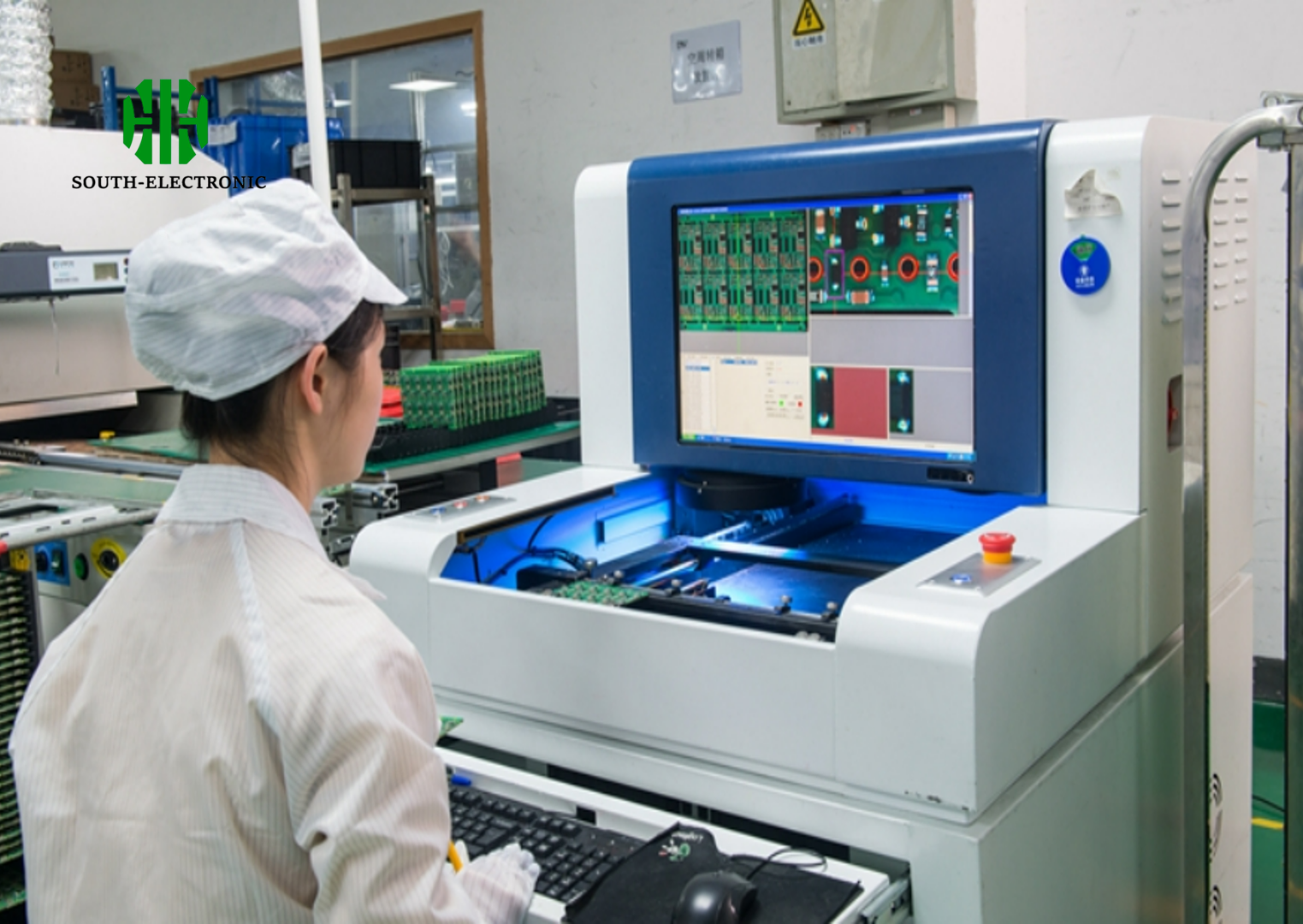
المشكلة 7: عدم كفاية الاختبار والتحقق
المشكلة:
تخطي مراحل الاختبار الشاملة يمكن أن يؤدي إلى ظهور مشكلات غير مكتشفة في المنتج النهائي.الحل:
قم بتنفيذ بروتوكول اختبار صارم يشمل المحاكاة البرمجية للأداء الكهربائي والاختبار الفعلي للموثوقية الحرارية والميكانيكية. استخدم أدوات مثل انعكاس المجال الزمني (TDR) لتحليل المقاومة، والتصوير الحراري لاكتشاف النقاط الساخنة وأداء الحرارة.
من خلال إدراك هذه الأخطاء الشائعة وتنفيذ الحلول المقترحة، يمكنك تحسين جودة وموثوقية تصميمات لوحات الدوائر المطبوعة متعددة الطبقات بشكل كبير. هذا النهج الاستباقي لا يحسن فقط من وظيفة منتجك ولكنه يقلل أيضًا من مخاطر التعديلات المكلفة وإعادة التصميم.
الفصل 9
اختبار وإصلاح المشكلات في لوحات الدوائر المطبوعة متعددة الطبقات
ضمان وظيفة وموثوقية لوحات الدوائر المطبوعة متعددة الطبقات يتطلب اختبارًا دقيقًا ومعالجة فعالة للمشكلات. إليك كيفية اختبار لوحاتك بشكل منهجي وحل المشكلات الشائعة بفعالية، لضمان تلبية منتجك لمعايير الأداء والمتانة.
اختبار لوحات الدوائر المطبوعة متعددة الطبقات
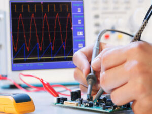
1. الاختبار الكهربائي:
اختبار التوصيلية:
يجب أن يكون هذا الخطوة الأولى. يتحقق من أن جميع التوصيلات في اللوحة تم إجراؤها بشكل صحيح وأنه لا توجد دوائر قصيرة. استخدم جهاز متعدد القياسات (Multimeter) أو معدات اختبار آلية (ATE) لفحص كل نقطة اتصال مقابل ملفات تصميم اللوحة.اختبار الدائرة الداخلية (ICT):
يعد هذا الاختبار أكثر شمولاً، حيث يتحقق من الدوائر القصيرة، الدوائر المفتوحة، المقاومة، السعة، والمعايير الكهربائية الأخرى التي يمكن أن تؤثر على وظيفة اللوحة. يتطلب الوصول الفعلي إلى جميع العقد، لذا خطط لنقاط اختبار في تصميمك.
2. الاختبار الوظيفي:
اختبار التشغيل:
قم بتشغيل اللوحة وراقب الاستجابات الأولية. تحقق من الفولتية المتوقعة في نقاط مختلفة وراقب أي سلوك غير متوقع مثل إعادة التعيين أو الفشل في البدء.اختبار سلامة الإشارة:
استخدم أجهزة قياس التذبذب (Oscilloscopes) ومحللات المنطق للتحقق من أن الإشارات عالية السرعة نظيفة وخالية من الضوضاء أو التشويه. هذا الاختبار مهم للدوائر التي تحتوي على مكونات عالية التردد.
3. الاختبارات البيئية:
دورات درجات الحرارة:
عرّض اللوحة لدرجات حرارة مختلفة للتأكد من قدرتها على تحمل الضغوط البيئية. يساعد ذلك في تحديد الفشل المحتمل الناتج عن التمدد الحراري.اختبار الرطوبة:
قم بمحاكاة بيئات ذات رطوبة عالية للتحقق من الأعطال المحتملة الناتجة عن التكثيف أو تسرب الرطوبة، والذي يمكن أن يسبب التآكل أو الدوائر القصيرة.
إصلاح المشكلات الشائعة في لوحات الدوائر المطبوعة1. الأعطال المتقطعة:
المشكلة:
تحدث عادةً بسبب وصلات لحام ضعيفة أو كسور دقيقة في المسارات.الحل:
استخدم عدسة مكبرة أو مجهرًا لفحص وصلات اللحام وأعد تدفق أي وصلات مشبوهة. يمكن أن يساعد التصوير الحراري في تحديد النقاط الساخنة التي تشير إلى وجود اتصال ضعيف.
2. مشاكل سلامة الإشارة:
المشكلة:
يمكن أن تسبب الضوضاء أو فقدان الإشارة أو تلف البيانات.الحل:
راجع ممارسات توجيه المسارات وحماية اللوحة. فكر في إضافة حماية إضافية أو إعادة توجيه المسارات لتقليل التداخل. تحقق من مطابقة المقاومة وتأكد من تنفيذ جميع نقاط الإنهاء بشكل صحيح.
3. المكونات المحمومة:
المشكلة:
يمكن أن تكون علامة على استهلاك تيار زائد أو إدارة حرارية غير كافية.الحل:
تحقق من أن شبكة توزيع الطاقة مصممة بشكل صحيح وأن جميع المكونات مناسبة للتيار الذي تتعامل معه. حسّن المسارات الحرارية باستخدام ثقوب إضافية أو تحسين تصميم المشتت الحراري.
4. مشاكل الطاقة:
المشكلة:
الفولتية غير الصحيحة أو تنظيم الطاقة غير السليم.الحل:
تحقق من أن جميع مصادر الطاقة توفر الفولتية الصحيحة وأن مكونات تنظيم الطاقة تعمل ضمن الحدود المحددة. استخدم مجس التيار لقياس استهلاك الطاقة الفعلي للوحة وتأكد من مطابقته للقيم المتوقعة.
5. الأخطاء الوظيفية:
المشكلة:
قد تكون ناتجة عن وضع المكونات بشكل غير صحيح، قيم مكونات غير صحيحة، أو أخطاء منطقية في تصميم الدائرة.الحل:
تحقق من جميع المكونات مقابل المخطط للتأكد من صحتها، وأعد التحقق من منطق الدائرة باستخدام أدوات المحاكاة.
توثيق العملية
احتفظ بسجل مفصل لجميع الاختبارات التي تم إجراؤها، بما في ذلك الظروف، النتائج، وأي حالات شاذة لوحظت. يعتبر هذا التوثيق ذا قيمة كبيرة لمعالجة المشاكل المتكررة وتحسين التصميمات المستقبلية.
الخلاصة
يُعد الاختبار ومعالجة المشكلات جزءًا أساسيًا من دورة حياة تصميم لوحات الدوائر المطبوعة. من خلال تطبيق هذه الممارسات بشكل منهجي، تضمن أن لوحات الدوائر المطبوعة متعددة الطبقات الخاصة بك ليست فقط قوية من الناحية الوظيفية ولكن أيضًا موثوقة عبر مختلف الظروف التشغيلية والبيئية. هذه الدقة لا تعزز جودة منتجك فحسب، بل تطيل أيضًا عمره الافتراضي في السوق.
الفصل 10
الاتجاهات المستقبلية في تصميم لوحات الدوائر المطبوعة متعددة الطبقات
مع استمرار تقدم التكنولوجيا، تتطور أيضًا تقنيات ومواد تصميم لوحات الدوائر المطبوعة. إليك نظرة على مستقبل تصميم لوحات الدوائر متعددة الطبقات، مع تسليط الضوء على الابتكارات التي قد تُحدث ثورة في كيفية التعامل مع هذه الأنظمة المعقدة.
1. لوحات الدوائر المرنة والقابلة للتمدد
تخيل لوحات دوائر يمكنها الانحناء، والمرونة، وحتى التمدد. من المتوقع أن توسع لوحات الدوائر المرنة والقابلة للتمدد إمكانيات تصميم الإلكترونيات، خاصة في التكنولوجيا القابلة للارتداء، والأجهزة الطبية، وحتى في التطبيقات الخاصة بالسيارات. تستخدم هذه اللوحات مواد مثل البولييميد أو الأفلام البوليسترية التي تسمح لها بالتكيف مع الأسطح غير التقليدية أو التحرك دون أن تنكسر. يفتح هذا التكيف آفاقًا جديدة لتصميم الأجهزة التي يجب أن تعمل في بيئات ديناميكية أو غير منتظمة.
2. أدوات التصميم المدعومة بالذكاء الاصطناعي
يغير الذكاء الاصطناعي والتعلم الآلي كيفية تصميم لوحات الدوائر المطبوعة. يمكن لأدوات التصميم المدعومة بالذكاء الاصطناعي أتمتة العمليات المعقدة مثل تخطيط التوصيلات وتوجيهها، مما يقلل بشكل كبير من وقت التصميم والأخطاء المحتملة. يمكن لهذه الأدوات تحليل كميات هائلة من البيانات لاقتراح تصاميم مثلى بناءً على معايير محددة مسبقًا، مثل تقليل الضوضاء أو خفض تكلفة المواد. مع تطور تكنولوجيا الذكاء الاصطناعي، ستقدم هذه الأدوات رؤى أكثر تطورًا، مما يبسّط عملية التصميم بشكل أكبر.
3. دمج المواد المتقدمة
يزداد استخدام المواد المتقدمة في لوحات الدوائر المطبوعة متعددة الطبقات. يتم استكشاف مواد مثل الغرافين والبوليمرات الموصلة لخصائصها الكهربائية والحرارية والميكانيكية الاستثنائية. على سبيل المثال، يوفر الغرافين توصيلًا كهربائيًا ممتازًا وقدرات عالية لإدارة الحرارة، مما قد يؤدي إلى لوحات تعمل بشكل أسرع وتبرد بشكل أكثر كفاءة. مع زيادة إتاحة هذه المواد، يمكن أن تحسن أداء ومتانة لوحات الدوائر بشكل كبير.
4. الطباعة ثلاثية الأبعاد للوحات الدوائر
من المتوقع أن تُحدث تقنية الطباعة ثلاثية الأبعاد تحولًا في تصنيع لوحات الدوائر، مما يمكن من التصنيع السريع للنماذج الأولية والتصاميم المعقدة متعددة الطبقات التي يصعب تحقيقها باستخدام الطرق التقليدية. تتيح الطباعة ثلاثية الأبعاد دمج المكونات الإلكترونية مباشرة في اللوحة أثناء عملية التصنيع، مما يقلل من وقت التجميع ويعزز من موثوقية اللوحات النهائية.
5. تطورات تقنية HDI (High Density Interconnect)
من المتوقع أن تستمر تقنية HDI، التي تتيح خطوطًا أرفع ومسافات أصغر وكثافة أعلى للمكونات، في التطور. قد تشمل التطورات المستقبلية ثقوبًا دقيقة أصغر ومواد تعبئة محسّنة للثقوب، مما يعزز الأداء الكهربائي وموثوقية اللوحة. سيكون ذلك ضروريًا لدعم الاتجاه المستمر نحو التصغير في الأجهزة الإلكترونية.
6. حلول إدارة الحرارة المتقدمة
مع تصغير المكونات وزيادة كثافة الطاقة، تصبح إدارة الحرارة في لوحات الدوائر متعددة الطبقات أكثر أهمية. تشمل الاتجاهات المستقبلية دمج تقنيات تبريد مبتكرة، مثل قنوات التبريد المدمجة أو الطبقات الحرارية الموصلة التي يمكنها سحب الحرارة بنشاط بعيدًا عن النقاط الساخنة. ستكون هذه الابتكارات ضرورية لأجهزة الحوسبة عالية الأداء والإلكترونيات ذات الطاقة العالية.
7. أدوات محاكاة واختبار أكثر تطورًا
توقع رؤية تحسينات في برامج المحاكاة التي يمكنها نمذجة السلوكيات الكهربائية والحرارية والميكانيكية بدقة أكبر. ستساعد هذه الأدوات المصممين على توقع كيفية أداء لوحات الدوائر المطبوعة متعددة الطبقات تحت ظروف مختلفة قبل تصنيعها فعليًا، مما يقلل من الحاجة إلى نماذج أولية متعددة ويساعد في ضمان أن المنتج النهائي يلبي جميع المواصفات.
الخلاصة
من خلال متابعة هذه الاتجاهات، يمكنك الاستعداد بشكل أفضل لمستقبل تصميم لوحات الدوائر المطبوعة متعددة الطبقات. سواء كان ذلك من خلال الاستفادة من مواد جديدة، أو استخدام أدوات الذكاء الاصطناعي، أو تبني تقنيات تصنيع مبتكرة، تعد هذه الابتكارات بتحسين قدرات وأداء لوحات الدوائر، مما يمكّن الجيل القادم من الأجهزة الإلكترونية.
تواصل معنا
أين نحن؟
الحديقة الصناعية، رقم 438 شارع دونغ هوان، رقم 438، شاجينغ دونغ هوان، منطقة باوان، شنتشن، قوانغدونغ، الصين
الطابق 4، مبنى زهيهوي الإبداعي، رقم 2005 شارع شيهوان، شاجينغ، منطقة باوان، شنتشن، الصين
الغرفة A1-13، الطابق 3، مركز يي ليم الصناعي، 2-28 شارع كواي لوك، كواي تشونغ، هونغ كونغ
service@southelectronicpcb.com
الهاتف: +86 400 878 3488
أرسل لنا رسالة
كلما كانت التفاصيل أكثر دقة، كلما تمكنا من المضي قدمًا إلى الخطوة التالية أسرع.

