
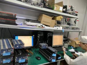
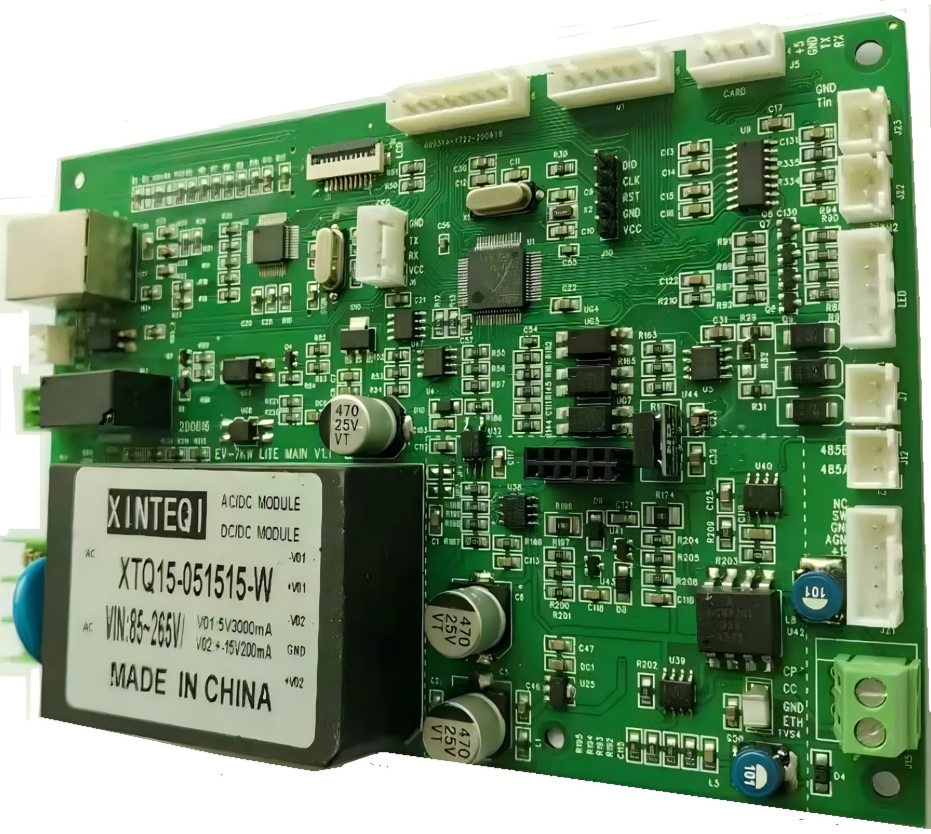
تصنيع نماذج PCB الأولية
South-Electronic
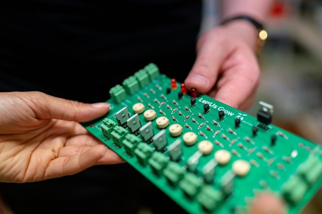
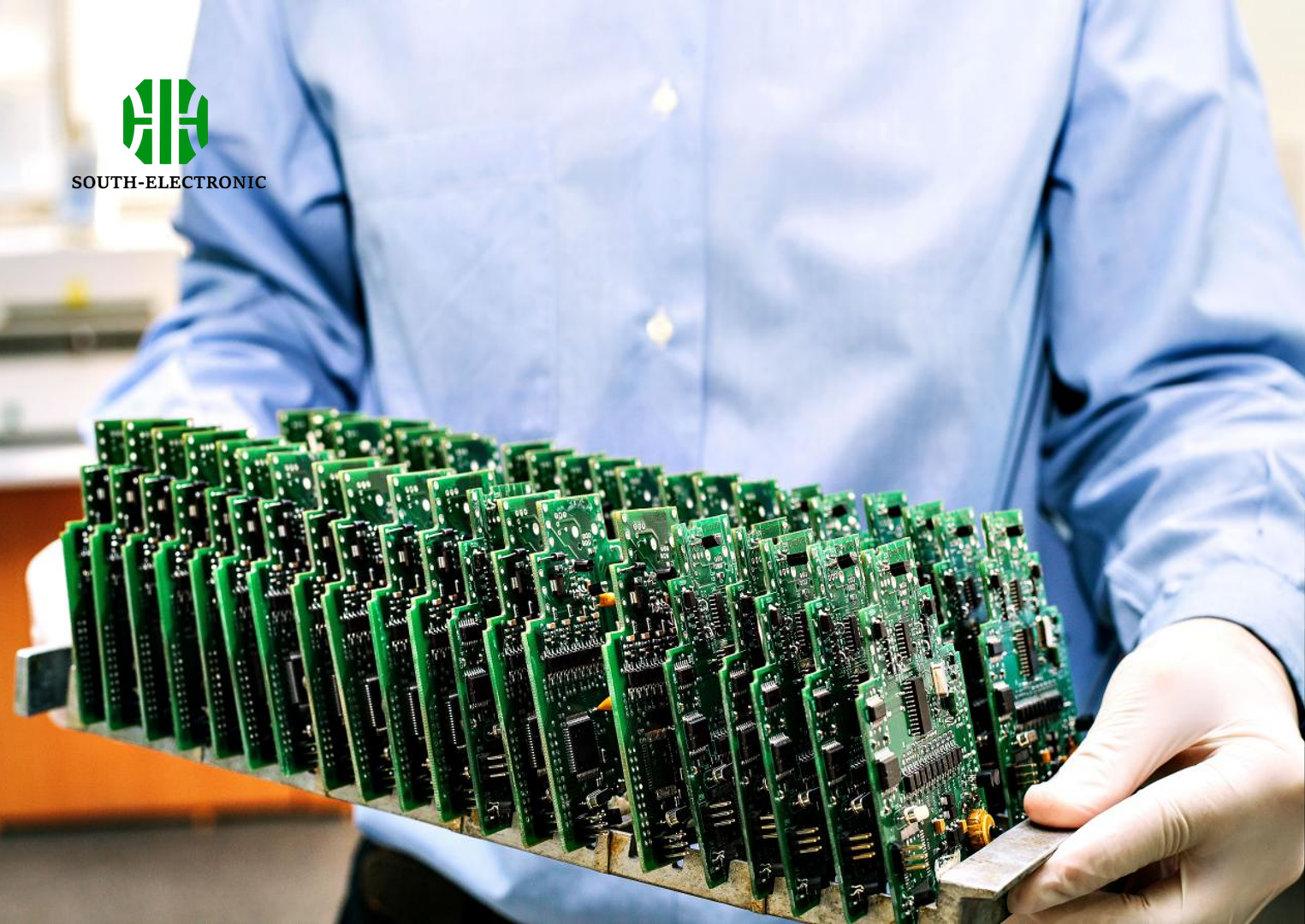
اختر South-Electronic للحصول على جودة لا تضاهى، واعتمادية، وقيمة استثنائية لتلبية احتياجاتك في تصنيع النماذج الأولية. اختبر الفرق مع خدمتنا المتكاملة – من الفكرة إلى المنتج النهائي، نضمن لك الدقة والسرعة والالتزام بمواصفاتك الفريدة.
مزودك الموثوق لخدمات تصنيع نماذج PCB الأولية
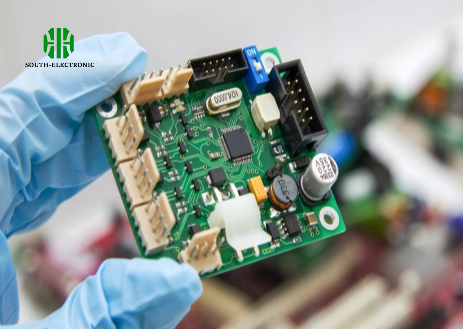
مرحبًا بك في South-Electronic، حيث تجد خدمات تصنيع نماذج PCB الأولية عالية الجودة والمعروفة بدقتها وسرعة تنفيذها.
تضمن نماذجنا الأولية أداءً فائقًا، مما يجعلها مثالية لاختبار مجموعة واسعة من التطبيقات قبل الإنتاج الكامل. استكشف تكوينات مختلفة مثل النماذج الأولية ذات الطبقة الواحدة، والطبقتين، والمتعددة الطبقات، والمصممة لتسريع عملية التطوير الخاصة بك.
لماذا تختار South-Electronic؟
-
مرونة في الطلب
اطلب ما تحتاجه بالضبط، في الوقت الذي تحتاجه.
سواء كنت تبحث عن نموذج أولي واحد أو عدة نسخ، نحن نخصص كل طلب لتلبية متطلباتك الفريدة، مما يضمن لك عملية مرنة وسلسة. -
فريق ذو خبرة
استفد من الخبرة الصناعية لمشروعك القادم.
مع أكثر من عقد من الخبرة، فريقنا هنا لمساعدتك على تحقيق النجاح من خلال الرؤى والمعرفة التي اكتسبناها من العمل في جميع أنحاء الصناعة. -
جودة مضمونة
تمتع بأفضل جودة مباشرة من المصنع.
باعتبارنا مصنعك الأساسي، نضمن لك جودة فائقة تفوق ما ستجده لدى الموردين الآخرين، مما يمنحك راحة البال التي تستحقها. -
تسليم سريع
احصل على طلباتك بسرعة مع عمليات الإنتاج الفعالة لدينا.
نحن ندرك أهمية الوقت. تضمن عملياتنا المبسطة وصول منتجاتك بسرعة، مما يبقي مشاريعك على المسار الصحيح دون تأخير. -
رضا مضمون
حلول PCB شاملة مصممة لتلبية رضاك.
مع مجموعة واسعة من معدات المعالجة، نقدم خدمات شاملة لتلبية جميع احتياجاتك من PCB، مما يضمن لك تجربة سلسة من البداية إلى النهاية.
المشاريع ذات الصلة التي قمنا بها
آراء العملاء
الأسئلة الشائعة
أكثر الأسئلة شيوعًا
Send us a message
The more detailed you fill out, the faster we can move to the next step.


الدليل الكامل لتصنيع نماذج PCB الأولية
المحتويات
الفصل 1
مقدمة عن تصنيع نماذج PCB الأولية
يُعتبر تصنيع نماذج PCB الأولية خطوة حاسمة في تطوير الأجهزة الإلكترونية. فهو يتيح للمصممين والمهندسين اختبار تصميماتهم الدائرية في ظروف واقعية قبل الانتقال إلى الإنتاج واسع النطاق. الهدف من تصنيع نماذج PCB الأولية هو إنشاء نسخة وظيفية مصغرة من المنتج النهائي، مما يساعد على تحديد أي عيوب في التصميم أو مشكلات كهربائية أو قيود ميكانيكية في وقت مبكر. من خلال اكتشاف المشكلات المحتملة في هذه المرحلة، يمكن للشركات توفير الوقت والمال مع ضمان أداء المنتج النهائي كما هو متوقع.
ما هو تصنيع نماذج PCB الأولية؟
يتضمن تصنيع نماذج PCB الأولية تصميم وإنتاج عدد محدود من لوحات الدوائر المادية للتحقق من وظائف التصميم. يساهم هذا في سد الفجوة بين مرحلتي المفهوم والإنتاج الضخم. يتيح التصنيع الأولي فرصة لاختبار كيفية تفاعل المكونات، تقييم سلامة مسارات الإشارة، وحل أي مشكلات محتملة في الأداء، وكل ذلك في بيئة صغيرة ومضبوطة. إنها عملية تكرارية تتطلب غالبًا عدة نسخ من النموذج الأولي قبل الوصول إلى تصميم نهائي جاهز للإنتاج.
لماذا يعتبر تصنيع نماذج PCB الأولية مهمًا؟
أهمية تصنيع نماذج PCB الأولية تتجلى في عدة أسباب:
- تقليل المخاطر: يساعد الكشف المبكر عن عيوب التصميم في تقليل مخاطر الأخطاء المكلفة خلال مرحلة الإنتاج.
- الاختبار والتحقق: يضمن التصنيع الأولي أن الدائرة تعمل كما هو مقصود في الظروف الواقعية، مما يحقق التحقق من الأداء الكهربائي والبنية الميكانيكية.
- تحسين التصميم: تتيح النماذج الأولية للمهندسين تجربة وضع المكونات، استراتيجيات التوصيل، وعناصر التصميم الأخرى لتحسين الأداء والتكلفة.
- تقليل الوقت للوصول إلى السوق: من خلال حل المشكلات في وقت مبكر من عملية التصميم، يتم تقليل الوقت الإجمالي اللازم لإطلاق المنتج في السوق، مما يجعل عملية التطوير أكثر كفاءة.
الفصل 2
اعتبارات التصميم
تصميم نموذج للوحة الدائرة المطبوعة (PCB) يتضمن العديد من القرارات الحاسمة التي تؤثر على الأداء والموثوقية والقابلية للتصنيع بالنسبة للنتاج النهائي. الحصول على التصميم الصحيح في المراحل الأولى من التصنيع النموذجي ضروري لضمان عمل اللوحة كما هو متوقع وتجنب الأعمال الإضافية الغالية في وقت لاحق. في هذا القسم ، سنغطي اعتبارات التصميم الرئيسية للوحة الدائرة المطبوعة التي يجب مراعاتها خلال مرحلة التصنيع النموذجي ، بما في ذلك وضع المكونات وتصميم المسارات والسلامة الإشاراتية وإدارة القدرة والقابلية للتصنيع.
1. وضع المكونات
أحد أولى وأهم خطوات تصميم لوحة الدائرة المطبوعة هو تحديد الموضع الأمثل للمكونات. يمكن لوضع المكونات الصحيح تحسين الأداء وتسهيل تصميم المسارات وضمان سهولة تجميع اللوحة وضمان صيانتها. هنا توجد إرشادات رئيسية للاتباع:
- مجموعة المكونات المرتبطة معًا: يجب وضع المكونات التي تعمل معًا بالقرب من بعضها البعض لتقليل طول المسارات وتقليل التأخيرات المحتملة للإشارات. على سبيل المثال ، يجب وضع المكثفات الفاصلة بالقرب من دبابيس الطاقة للمكثفات المتكاملة لفلاتر الضوضاء بكفاءة.
- وضع المكونات الحساسة استراتيجيًا: يجب وضع المكونات التناظرية والدوائر عالية التردد والمكونات الحساسة مثل الأجهزة المذبذبة بعيدًا عن الدوائر الرقمية الصاخبة لتجنب التداخل.
- النظر في إدارة الحرارة: يجب وضع المكونات التي تنتج الحرارة ، مثل المنظمات أو الترانزستورات القوية ، بشكل منفصل لتجنب ارتفاع درجة الحرارة. يجب التأكد من وجود مساحة كافية لمنفذ الحرارة أو الفيوز الحرارية لإدارة التبديد الحراري بشكل فعال.
- اتجاه المكونات: من أجل تسهيل التجميع ، يجب تحديد اتجاه المكونات بشكل متسق ، خاصةً إذا كنت تستخدم آلات التجميع الآلية. هذا يقلل من فرصة الخطأ خلال عملية التجميع.
2. تصريف المسارات
تصريف المسارات أمر بالغ الأهمية لضمان سلامة الإشارات والاتصالات الكهربائية الموثوقة على لوحة الدائرة المطبوعة. يمكن لتصريف المسارات السيئ أن يؤدي إلى تدهور الإشارات والضوضاء وحتى فشل الدائرة .
- النقاط الرئيسية للنظر فيها: تقليل طول المسارات: تقليل طول المسارات يقلل من المقاومة والتحريض ، مما يساعد على الحفاظ على جودة الإشارات. الإشارات عالية التردد أو الإشارات السريعة ، يمكن أن تسبب المسارات الأطول تأخيرات أو انعكاسات للإشارات ، لذا يجب الحفاظ على أقصر مسار ممكن.
- اتباع قاعدة 90/45 درجة: تجنب الزوايا الحادة 90 درجة عند تصريف المسارات ، لأنها يمكن أن تسبب انعكاسات الإشارات وتداخل كهرومغناطيسي. بدلاً من ذلك ، استخدم منعطفات 45 درجة لتحسين تدفق الإشارات.
- استخدام مسارات واسعة للخطوط الجهد: يجب أن تكون مسارات الجهد ، خاصةً تلك التي تحمل تيارات أعلى ، أكثر عرضًا من مسارات الإشارات لتقليل انخفاض الجهد وتجنب ارتفاع درجة الحرارة. يمكنك استخدام حاسبات عرض المسار عبر الإنترنت لتحديد العرض الصحيح بناءً على مستويات التيار.
- المواصفات المحددة: التصميمات عالية السرعة أو التصميمات الراديوية ، يجب الحفاظ على مواصفات محددة على طول المسارات. غالبًا ما يتطلب هذا النظر بعناية في عرض المسار والفاصل والматериال العازل المستخدم في لوحة الدائرة المطبوعة.
3. مسارات الأرض والقدرة
التركيب الصحيح للأرض والقدرة ضروري لمنع الضوضاء وتقلبات الجهد وتدهور الإشارات في تصميم لوحة الدائرة المطبوعة. بعض النقاط للنظر فيها تشمل:
- مسار أرض مخصص: يوفر مسار أرض مستمر في لوحة الدائرة المطبوعة متعددة الطبقات مسار منخفض المقاومة للتيارات العائدة ويقلل من التداخل الكهرومغناطيسي. كما يساعد على تحسين سلامة الإشارات ويقلل من فرصة ربط الضوضاء.
- مسار القدرة: يوصى بمسار قدرة منفصل لتوفير مصدر طاقة مستقر لجميع المكونات. هذا يقلل من المقاومة والتحريض المرتبطين بالمسارات التقليدية للطاقة وي في الحفاظ على مستويات الجهد الثابتة.
- المكثفات الفاصلة: استخدم المكثفات الفاصلة لفلاتر الضوضاء من مصدر الطاقة. يجب وضعها بالقرب من دبابيس الطاقة للمكثفات المتكاملة لتكون الأكثر فعالية.
- تركيب أرض النجم:对于 الدوائر التناظرية الحساسة ، يُفضل تركيب أرض النجم لتجنب حلقات الأرض ، حيث يكون لكل دائرة فرعية طريقها الخاص إلى الأرض الرئيسية ، وتمنع التداخل بين الدوائر.
4. سلامة الإشارات وإدارة التداخل الكهرومغناطيسي
تُشير سلامة الإشارات إلى جودة ودقة الإشارات الكهربائية التي تعبر لوحة الدائرة المطبوعة. كما أن إدارة التداخل الكهرومغناطيسي ضرورية لتجنب تدهور الإشارات. النقاط الرئيسية للنظر فيها تشمل:
- احتفظ بالإشارات السريعة отдель: يمكن أن تسبب الإشارات السريعة تداخل كبيرًا وتداخل. لتقليل التداخل ، احتفظ بهذه الإشارات بعيدًا عن الإشارات الحساسة الأخرى باستخدام تقنيات العزل مثل الحماية أو الفصل بالمسافة.
- تصميم المسارات الزوجية التفاضلية: الإشارات السريعة مثل USB أو HDMI ، استخدم تصميم المسارات الزوجية التفاضلية ، حيث يتم توجيه إشارات مكملة معًا لإلغاء الضوضاء. تأكد من أن هذه المسارات متساوية الطول لتجنب انزياح الإشارات.
- إنهاء الإشارات: استخدم مقاومات الإنهاء المناسبة لمطابقة المقاومة للمسارات الإشارات السريعة. هذا يمنع انعكاسات الإشارات و يحافظ على سلامة الإشارات على مسارات أطول.
- وضع فيا الأرض: استخدم فيا الخياطة لربط مسارات الأرض عبر الطبقات المتعددة. هذا يساعد على تقليل الضوضاء التردد العالي ويضمن مرجع أرض مستقر في جميع أنحاء لوحة الدائرة المطبوعة.
5. إدارة الحرارة
تُعتبر إدارة الحرارة فعالة أمرًا بالغ الأهمية ، خاصةً لوحات الدائرة المطبوعة التي تحتوي على مكونات قوية أو تيار عالي. يمكن أن يؤدي ارتفاع درجة الحرارة إلى فشل المكونات أو تدهور الأداء مع مرور الوقت. النقاط الرئيسية للنظر فيها تشمل:
- فيات الحرارة:对于 المكونات التي تنتج حرارة كبيرة ، استخدم فيات الحرارة لنقل الحرارة بعيدًا عن المكون إلى مناطق أخرى من اللوحة أو إلى منفذ حراري.
- منفذ الحرارة والألواح الحرارية: قد تتطلب المكونات مثل منظمات الجهد أو الترانزستورات القوية منفذ حراري أو ألواح حرارية لتالحرارة بكفاءة. تأكد من وجود مساحة كافية على اللوحة لاستيعاب هذه الميزات.
- مسافة المكونات: يمكن أن تحسن المسافة الصحيحة بين المكونات من تدفق الهواء ، خاصةً في التصميمات التي تستخدم تبريد الهواء القسري. يمكن أن يؤدي إ tắc المكونات إلى حبس الحرارة وحدوث بقع ساخنة محلية.
الختام
عند تصميم نموذج للوحة الدائرة المطبوعة ، يجب النظر بعناية في وضع المكونات وتصميم المسارات وأرضيته والقدرة و سلامة الإشارات والقابلية للتصنيع. لكل من هذه العوامل دور حاسم في ضمان عمل لوحة الدائرة المطبوعة بكفاءة و التوقعات الأدائية ويمكن إنتاجها بتكلفة معقولة. من خلال معالجة هذه الاعتبارات التصميمية في مرحلة مبكرة من عملية التصنيع النموذجي ، يمكنك إنشاء لوحة دائرة مطبوعة لا تعمل فقط ولكنها أيضًا قابلة للتوسع لإنتاج الكتلة ، مما يساعدك على تحقيق وقت سوق أسرع ومنتج نهائي أكثر موثوقية.
الفصل 3

نصائح حول تصميم لوحة الدائرة المطبوعة
إن تصميم لوحة دائرة مطبوعة جيدة أمر حيوي لنجاح النموذج الأولي. إنه يضمن وظائف موثوقة وتصنيعًا وأداءً. هنا بعض النصائح المهمة لتحسين تصميم لوحة الدائرة المطبوعة أثناء مرحلة النمذجة الأولية:
تحسين موقع المكونات
تسلسل المسارات
- مسارات قصيرة ومباشرة: احتفظ بالمسارات قصيرة لتقليل المقاومة وتحسين صحة الإشارة.
- تجنب الزوايا القائمة: استخدم زوايا 45 درجة لتقليل التداخل الكهرومغناطيسي والانعكاس الإشارات.
- عرض المسار الصحيح: تأكد من أن مسارات الطاقة واسعة بما يكفي для التعامل مع التيار دون ارتفاع درجة الحرارة.
مسارات الأرض والطاقة
- مسار أرض مخصص: استخدم مسارًا أرضيًا كامل الطبقة لتقليل الضوضاء وتحسين صحة الإشارة.
- مسار الطاقة: تأكد من وجود مصدر طاقة مستقر باستخدام مسار طاقة مخصص ، مما يقلل من الحث والتسرب.
صحة الإشارة
- إشارات عالية السرعة: أعد توجيه إشارات عالية السرعة أولاً واستخدم توجيه الأزواج المتفاوتة حيث يلزم الأمر. احتفظ بهذه المسارات قصيرة وبعيدة عن مصادر الضوضاء.
- مراقبة.Impedance: للتصاميم عالية التردد ، تأكد من أن المسارات تحتفظ بالتحكم المحدد في الضوضاء لتجنب فقدان الإشارة.
إدارة الحرارة
- مسالك حرارية: استخدم مسالك حرارية لت الحرارة من المكونات القوية.
- مساحات النحاس: اشتمل على مساحات كبيرة من النحاس للمساعدة في تقليل الحرارة وتثبيت درجة الحرارة.
تصميم قابل للتصنيع
- مكونات معيارية: استخدم أحجام المكونات الشائعة لتقليل التكاليف وتسهيل التجميع.
- مسافة كافية: تأكد من وجود مساحة كافية بين المسارات والمكونات لتجنب القصارات أو مشاكل التجميع.
- نقاط الاختبار: اشتمل على نقاط اختبار لتحليل الأخطاء بسهولة أثناء مرحلة النمذجة الأولية.
القيود الميكانيكية
- شكل و حجم اللوحة: تأكد من أن لوحة الدائرة المطبوعة تتناسب مع غلافها ، مع وجود مساحة للوصلات وثقوب التثبيت.
- موقع الوصلات: ضع الوصلات على الحافة للوصول السهل ، مع التأكد من وجود مساحة كافية للاتصالات الخارجية.
الخلاصة
متابعة نصائح تصميم لوحة الدائرة المطبوعة أثناء مرحلة النمذجة الأولية تساعد على ضمان تصميم موثوق ووظيفي ويمكن تصنيعه. التخطيط الصحيح ، والتوجيه الفعال ، والاعتبار المتعمد للعوامل المتعلقة بالطاقة والحرارة والميكانيكية هي المفتاح لتصميم لوحة دائرة مطبوعة ناجحة.
الفصل 4
Material Selection
The materials used in PCB must be carefully selected to withstand the environmental challenges of automotive applications. Common materials include:
- FR-4: The most widely used substrate due to its durability and cost-effectiveness.
- Polyimide: Known for its flexibility and heat resistance, suitable for high-temperature applications.
- Aluminum: Offers excellent heat dissipation and is commonly used in LED lighting and power supplies. Choosing the right materials helps in achieving the desired durability and functionality while keeping costs in check.
الفصل 5

Prototyping Tools and Techniques
Various software tools are available for PCB design, such as Altium Designer, Eagle, and KiCAD. These tools help in laying out the board and simulating its behavior before manufacturing. Choosing the right tool depends on the complexity of the project and the designer’s familiarity with the software.
الفصل 6
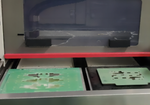
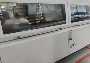
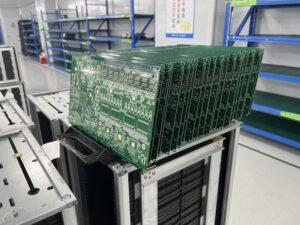
Manufacturing the Prototype
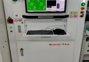
Choosing the right manufacturer is crucial for a successful PCB prototype. It’s important to select a vendor that can handle the specific requirements of your project, whether it involves special materials, tight tolerances, or complex multilayer structures.
الفصل 7

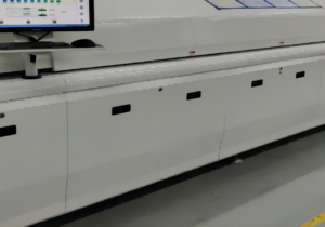
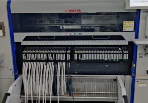
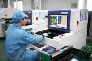
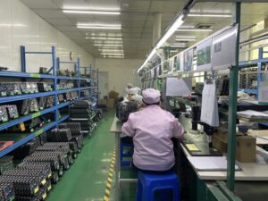
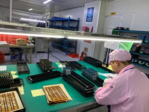
Assembly Techniques
The assembly of a PCB prototype involves various techniques. Manual soldering is common for small batches or simple prototypes. For more complex boards, reflow soldering might be used, which involves placing solder paste and components on the board and then heating it to form solder joints.
الفصل 8
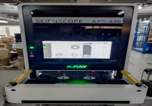
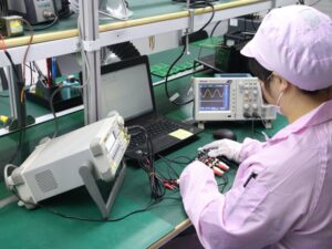
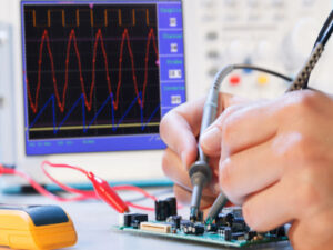
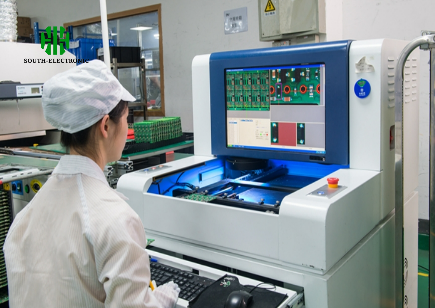
Testing and Debugging
Testing a PCB prototype is crucial to validate its functionality. This can involve functional tests, where the board is powered up and checked for correct operation, and electrical tests, such as continuity and isolation resistance tests.
الفصل 9
Iteration and Refinement
After testing, the prototype might require changes. This iterative process is vital to refining the design. Feedback from testing is used to modify the design and improve the product. This cycle continues until the prototype meets all the desired specifications and functions correctly.
الفصل 10
Finalizing the Design for Production
Once the prototype is finalized and fully tested, it’s time to prepare for production. This involves finalizing the design files, creating a bill of materials (BOM), and writing assembly instructions.
Documentation is crucial to ensure a smooth transition to mass production. It’s also important to select a manufacturer who can scale from prototype to full production in terms of capacity and quality control.
This comprehensive guide should provide a robust foundation for anyone involved in PCB prototyping, whether they are new to the field or are experienced professionals looking to refine their process.
Get in touch
Where Are We?
Industrial Park, No. 438 Donghuan Road, No. 438, Shajing Donghuan Road, Bao'an District, Shenzhen, Guangdong, China
Floor 4, Zhihui Creative Building, No.2005 Xihuan Road, Shajing, Baoan District, Shenzhen, China
ROOM A1-13,FLOOR 3,YEE LIM INDUSTRIAL CENTRE 2-28 KWAI LOK STREET, KWAI CHUNG HK
service@southelectronicpcb.com
Phone : +86 400 878 3488
Send us a message
The more detailed you fill out, the faster we can move to the next step.

