
Tiny holes, big impact. Modern electronics demand smaller, faster, and more reliable connections. Without microvias, your smartphone would look like a 1980s brick – and perform just as poorly.
HDI PCB microvias[^1] are essential for compact, high-speed devices. They enable thinner circuit boards, faster signal transmission, and better thermal management compared to traditional through-holes – critical for 5G phones, smartwatches, and IoT devices working in tight spaces.
Let’s drill down into why these microscopic tunnels are reshaping electronics manufacturing – and what engineers need to know about their capabilities and limitations.
What Exactly Are HDI PCB Microvias?
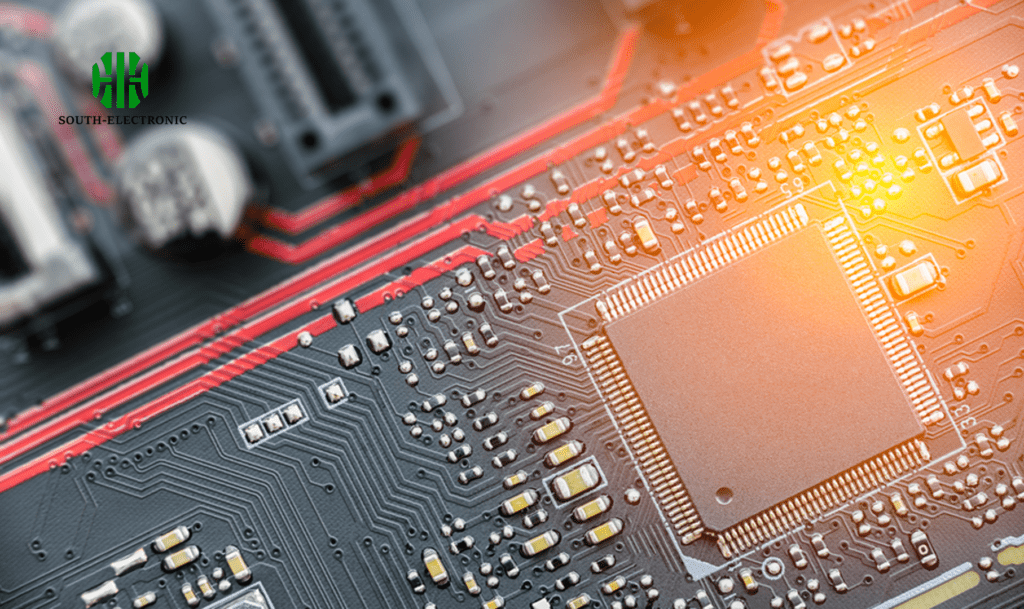
Stop picturing old-school drill holes. The copper-plated microvias in HDI boards are laser-made tunnels – smaller than a human hair – connecting different circuit layers in advanced PCBs.
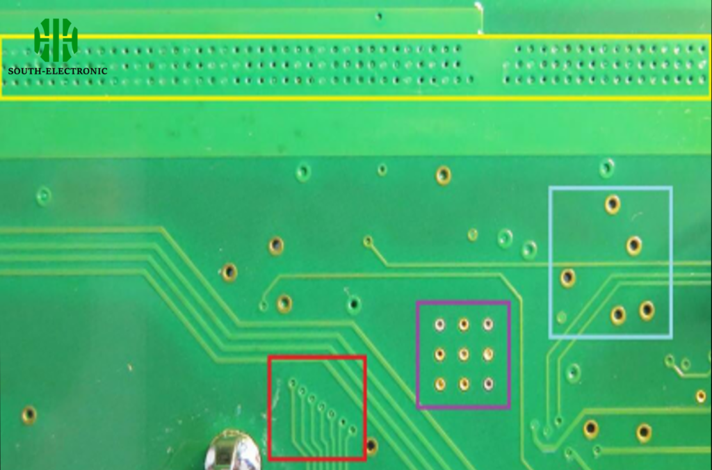
Microvias are laser-drilled, copper-filled vertical connections (typically <150µm diameter) that create pathways between layers in high-density interconnect PCBs. They come in blind, buried, stacked, and staggered configurations for dense component packing.
)
Three Key Microvia Variations
Microvias solve specific design challenges:
-
Blind Microvias[^2]
Connect outer layers to first inner layer
Diameter: 50-100µm
Depth: ≤1:1 aspect ratio -
Buried Microvias[^3]
Link inner layers without surfacing
Require sequential lamination
Enables complex 12+ layer boards -
Stacked vs Staggered
| Type | Space Efficiency | Reliability Risk | Typical Use |
|---|---|---|---|
| Stacked | Highest | Thermal stress | Ultra-compact designs |
| Staggered | Moderate | Lower failure rate | High-reliability applications |
Staggered configurations (offset between layers) improve mechanical stability, while stacked versions (direct vertical alignment) maximize space savings for wearables.
Why Are Microvias Better Than Traditional Through-Hole Vias?
Imagine trying to park an SUV in a motorcycle spot. That's traditional through-hole vias in modern PCBs – bulky and space-wasting.
Microvias save up to 70% space vs through-hole vias. Their smaller size reduces signal path lengths (critical for 25+ GHz signals) and improves thermal dissipation – enabling complex routing under BGA packages.
)
Head-to-Head Performance Comparison
| Feature | Microvias | Through-Hole Vias |
|---|---|---|
| Typical Diameter | 15-150µm | 300-600µm |
| Aspect Ratio | ≤1:1 | Up to 10:1 |
| Signal Delay | 0.3-1.2ps | 2-5ps |
| Space Efficiency | 8-10 vias/mm² | 1-2 vias/mm² |
| Thermal Resistance | 15-25°C/W | 30-50°C/W |
The tighter aspect ratios prevent plating voids during manufacturing. For 0.4mm pitch BGAs, only microvias provide sufficient escape routing density.
Do Microvias Improve Signal Integrity in High-Speed Designs?
Signal degradation at 28GHz+ turns PCB traces into radio antennas. Microvias act like traffic cops – directing signals efficiently without interference.
Properly designed microvias reduce reflection by 60% vs through-holes in 5G/mmWave circuits. Their shorter vertical spans minimize impedance discontinuities and capacitive coupling between layers.
Four Signal Integrity[^1] Factors
-
Reduced Stub Effects
Through-holes create unused via portions (stubs) causing signal reflections. Microvias' shallow depth (≤100µm) eliminate this issue above 10GHz. -
Controlled Impedance
Laser precision enables ±5% impedance control via:- Tighter diameter tolerance (±5µm vs ±50µm)
- Smohether copper plating
-
Crosstalk Mitigation
Tighter via spacing (150-200µm pitch) allows better ground shielding between high-speed differential pairs. -
Material Compatibility
Works with low-Dk/Df dielectrics like Megtron 6 and FR408HR for 112G PAM4 signals.
How Small Can Microvias Be? Design Limitations Explained
Pushing microvia limits is like balancing on a razor's edge – go too small and reliability plummets.
Current production microvias reach 15µm diameter with 20µm pad size. Practical limits are 50µm diameter (mechanical drilling) and 25µm (laser) – constrained by copper plating quality and dielectric strength.
Technical Barriers and Solutions
| Limitation Factor | Current Capability | Breaking Point | Mitigation Strategy |
|---|---|---|---|
| Laser Accuracy | ±3µm | <10µm beam spot | UV lasers vs CO2 |
| Aspect Ratio | 1:1 (0.8:1 optimal) | 1.2:1 failures | Depth-controlled drilling |
| Plating Void Risk | 15% at 30µm | Pulse reverse plating | |
| Thermal Cycling | 1000 cycles @ -55/+125°C | Delamination @ 1500+ | Low-CTE dielectrics |
For 800+ layer counts in AI accelerator boards, staggered 50µm microvias with 3µm copper achieve 15+ year lifespan under 85°C/85% RH conditions.
Are Microvias Reliable Enough for Long-Term Use?
A board fails mid-surgery – nightmare fuel. But modern microvias pass 1000+ thermal cycles in qualification tests.
Automotive-grade microvias demonstrate 0.02% failure rate over 15 years. Advanced direct metallization (M-SAP) and filled via-in-pad techniques prevent cracks under -55°C to 150°C thermal shock.
)
Five Reliability Enhancers
-
Material Selection
High Tg (>180°C) dielectrics like Isola Astra MT77 minimize Z-axis expansion. -
Plating Process
Electroless copper + pulse plating achieves 12µm ductile copper walls (vs 5µm brittle plating). -
Filling Options
Conductive (silver epoxy) or non-conductive (resin) fills prevent voids:Fill Type Thermal Conductivity Cost Best For Conductive 65 W/mK High Thermal hot spots Non-Conductive 0.3 W/mK Medium General purpose -
Design Rules
- 300µm keep-out from board edge
- 2:1 pad-to-via ratio
- No via-in-pad for >5mm² components
-
Testing Protocols
6-layer daisy chain test coupons verify 8kV HALT compliance pre-production.
Conclusion
HDI microvias enable smarter, smaller devices from pacemakers to satellite comms. With 5µm laser capabilities emerging, they’ll continue driving electronics miniaturization while meeting stringent automotive/aerospace reliability demands.
[^1]: Explore how HDI PCB microvias enhance device performance and design flexibility, crucial for modern electronics.
[^2]: Learn about blind microvias and their role in connecting layers efficiently in high-density PCBs.
[^3]: Discover the advantages of buried microvias for complex PCB designs and their impact on performance.
[^4]: Learn about the critical role of Microvias in maintaining Signal Integrity for advanced PCB designs, especially in 5G technology.

