

The manufacturability of PCB design is divided into two categories:
- It refers to the processing technology of producing printed circuit boards;
- It refers to the assembly technology of components and printed circuit boards on circuits and structures.
For the processing technology of printed circuit boards, general PCB manufacturers, due to their manufacturing capabilities, will provide designers with relevant requirements in great detail, and the application situation is relatively good in practice. According to the author’s understanding, the second category, that is, manufacturability design for electronic assembly, has not received enough attention in practice.
The focus of this article is also to describe the manufacturability issues that designers must consider during the PCB design stage.
How to choose the assembly method and component layout appropriately?
The selection of assembly method and component layout is a very important aspect of PCB manufacturability, which has a great impact on assembly efficiency, cost and product quality. In fact, the author has come into contact with quite a lot of PCBs, and some very basic principles are still lacking.
- Choose a suitable assembly method
Usually, for different assembly densities of PCBs, the recommended assembly methods are as follows:

As a circuit design engineer, you should have a correct understanding of the assembly process of the designed PCB, so as to avoid making some principled mistakes. When choosing an assembly method, in addition to considering the assembly density of the PCB and the difficulty of wiring, you must also consider the typical process flow of this assembly method and the level of the company’s own process equipment. If the company does not have a good wave soldering process, then choosing the fifth assembly method in the above table may bring you a lot of trouble.
Another point worth noting is that if you plan to implement a wave soldering process on the welding surface, you should avoid arranging a few SMDs on the welding surface to complicate the process.
- Component layout
The layout of components on the PCB has a significant impact on production efficiency and cost, and is an important indicator for measuring the assemblability of the PCB design. Generally speaking, components are arranged as evenly, regularly, and neatly as possible, and are arranged in the same direction and polarity. Regular arrangement facilitates inspection, which is conducive to improving the speed of patch/plug-in, and uniform distribution is conducive to heat dissipation and optimization of welding process.
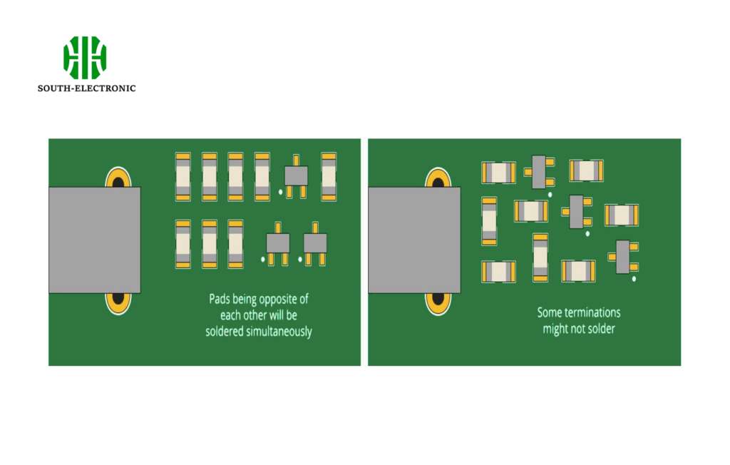
On the other hand, to simplify the process flow, PCB designers should always be aware that only one of the group soldering processes, reflow soldering and wave soldering, can be used on any side of the PCB. This is especially noteworthy when the assembly density is high and more SMD components must be distributed on the soldering surface of the PCB.
Designers should consider which group soldering process to use for the SMD components on the soldering surface. The most preferred is to use the wave soldering process after the SMD is cured, which can simultaneously solder the pins of the through-hole components on the component surface; however, wave soldering of SMD components has relatively strict constraints and can only solder chip resistors and capacitors, SOT, and SOIC of 0603 and above (pin spacing ≥1mm and height less than 2.0mm).
For components distributed on the soldering surface, the direction of the pins should be perpendicular to the transmission direction of the PCB during wave soldering to ensure that the solder terminals or leads on both sides of the components are dipped at the same time. The arrangement order and spacing between adjacent components should also meet the requirements of wave soldering to avoid the "shielding effect", as shown in Figure 1. When wave soldering is used for multi-pin components such as SOIC, tin stealing pads should be set at the last two (1 on each side) solder feet in the direction of tin flow to prevent continuous soldering.

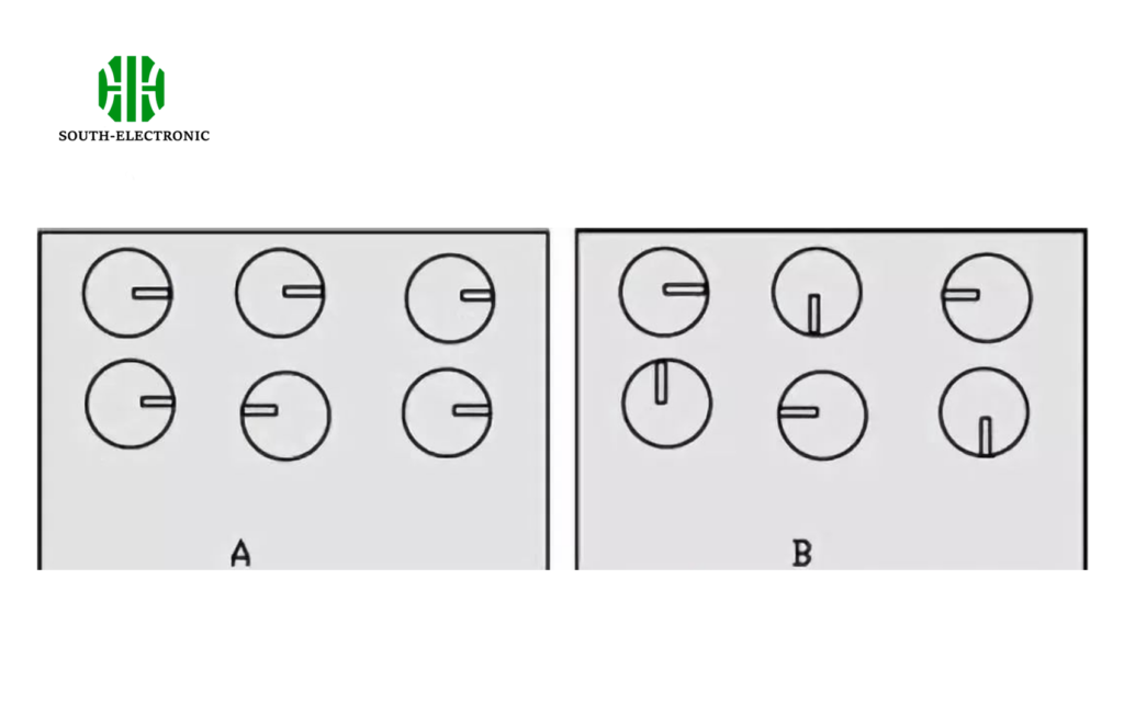
Components of similar types should be arranged in the same direction on the board to make it easier to mount, inspect and solder the components. For example, make the negative poles of all radial capacitors face the right side of the board, make the notch marks of all dual in-line packages (DIP) face the same direction, etc. This can speed up the insertion and make it easier to find errors.
As shown in the figure below, since board A uses this method, it is easy to find the reverse capacitor, while board B takes more time to find. In fact, a company can standardize the direction of components on all circuit boards it manufactures. The layout of some boards may not necessarily allow this, but this should be a direction to strive for.
Also, similar component types should be grounded together as much as possible, with the first pin of all components in the same direction, as shown below:
But I have indeed encountered quite a few PCBs with too high assembly density. Tantalum capacitors, chip inductors and other high-level components and fine-pitch SOIC, TSOP and other devices must also be distributed on the soldering surface of the PCB. In this case, only double-sided printing of solder paste can be used for patch reflow soldering, and plug-in components should be distributed as concentrated as possible to accommodate manual soldering.
Another possibility is that the perforated components on the component surface should be distributed on several main straight lines as much as possible to accommodate the latest selective wave soldering process, which can avoid manual soldering and improve efficiency and ensure soldering quality. Discrete solder point distribution is a taboo for selective wave soldering, which will double the processing time.
When adjusting the position of components in the printed circuit board file, it is important to pay attention to the one-to-one correspondence between components and silk-screen symbols. If the component is moved without correspondingly moving the silk-screen symbol next to the component, it will become a major quality risk in manufacturing, because in actual production, silk-screen symbols are industry languages that guide production.
Clamping edges, positioning marks, and process positioning holes for automated production must be arranged on the PCB
At present, electronic assembly is one of the industries with the highest degree of automation. The automated equipment used in production requires automatic transmission of PCBs. This requires that there should be a clamping edge of no less than 3-5mm wide on the top and bottom of the PCB in the transmission direction (generally the long side direction) to facilitate automatic transmission and avoid the components near the edge of the board from being unable to be automatically assembled due to clamping.
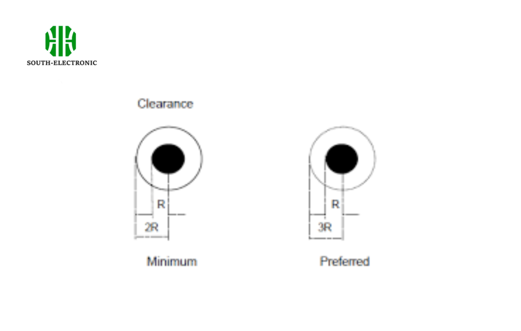
The role of the positioning mark is that for the assembly equipment that currently widely uses optical positioning, the PCB needs to provide at least two or three positioning marks for the optical recognition system to accurately locate the PCB and correct the processing error of the PCB. Among the commonly used positioning marks, two marks must be distributed on the diagonal lines of the PCB. The selection of positioning marks generally uses standard graphics such as solid circular pads. For easy identification, there should be an open area around the mark without other circuit features or marks. The size should preferably not be less than the diameter of the mark (as shown in Figure 4), and the mark should be more than 5mm away from the edge of the board.
In the manufacturing of the PCB itself, as well as in the semi-automatic plug-in, ICT testing and other processes in the assembly, the PCB needs to provide two to three positioning holes at the corners.
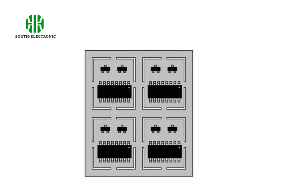
Reasonable use of paneling to improve production efficiency and flexibility
When assembling PCBs with small or irregular dimensions, there are many restrictions, so the general method of paneling is to splice several small PCBs into a PCB of appropriate size for assembly, as shown in Figure 5. Generally, PCBs with a single side size of less than 150mm can consider the paneling method. Through two, three, four, etc., the size of the large PCB can be spliced to the appropriate processing range. Usually, PCBs with a width of 150mm~250mm and a length of 250mm~350mm are more suitable sizes for automated assembly.
Another way to splice panels is to splice PCBs with SMDs on both sides into a large board, which is commonly known as Yin-Yang splicing. It is generally done to save the cost of stencils, that is, through such splicing, only one stencil is needed instead of two. In addition, when technicians compile the operation program of the placement machine, the PCB programming efficiency of Yin-Yang splicing is also higher.
When splicing panels, the connection between sub-boards can be made by double-sided V-grooves, long slots and round holes, etc., but when designing, it is necessary to consider making the separation line in a straight line as much as possible to facilitate the final separation. At the same time, it is also necessary to consider that the separation edge should not be too close to the PCB routing, which makes it easy to damage the PCB during the separation.
There is also a very economical splicing, which does not refer to splicing PCBs, but splicing the mesh patterns of stencils. With the application of fully automatic solder paste printers, the more advanced printers now allow the opening of multi-sided PCB mesh patterns on a steel mesh with a size of 790×790mm, so that one steel mesh can be used for printing multiple products. This is a very cost-saving approach, especially suitable for manufacturers with small batches and multiple varieties of products.
Considerations for testability design
The testability design of SMT is mainly aimed at the current ICT equipment situation. The test issues of later product manufacturing are taken into account when designing circuits and surface mounted printed boards (SMBs). To improve testability design, the requirements of both process design and electrical design should be considered.
- Requirements for process design
The positioning accuracy, substrate manufacturing procedures, substrate size, and probe type are all factors that affect detection reliability.
- Accurate positioning holes. Set accurate positioning holes on the substrate, and the positioning hole error should be within ±0.05mm. At least two positioning holes should be set, and the farther the distance, the better. Use non-metallized positioning holes to reduce the thickening of the solder coating and fail to meet the tolerance requirements. If the substrate is manufactured as a whole piece and then tested separately, the positioning holes must be set on the main board and each separate substrate.
- The diameter of the test point should not be less than 0.4mm, and the spacing between adjacent test points should preferably be above 2.54mm and not less than 1.27mm.
- Components with a height exceeding *mm cannot be placed on the test surface. Components that are too high will cause poor contact between the online test fixture probe and the test point.
- It is best to place the test point 1.0mm away from the component to avoid collision damage between the probe and the component. There should be no components or test points within 3.2mm around the positioning hole ring.
- The test point cannot be set within 5mm of the PCB edge. This 5mm space is used to ensure fixture clamping. Usually, the same process edge is also required in conveyor belt production equipment and SMT equipment.
- All detection points are preferably tinned or use metal conductors with a softer texture, easy to penetrate, and not easy to oxidize to ensure reliable contact and extend the service life of the probe.
- The test point cannot be covered by solder mask or text ink, otherwise the contact area of the test point will be reduced, reducing the reliability of the test.
- Electrical design requirements
- It is required to lead the test point of SMC/SMD on the component surface to the welding surface through vias as much as possible, and the diameter of the via should be greater than 1mm. This allows the online test to be tested using a single-sided needle bed, thereby reducing the cost of online testing.
- Each electrical node must have a test point, and each IC must have test points for POWER and GROUND, and they must be as close to the component as possible, preferably within 2.54mm from the IC.
- When setting test points on the circuit traces, their width can be enlarged to 40mil wide.
- Evenly distribute the test points on the printed circuit board. If the probes are concentrated in a certain area, the higher pressure will deform the board to be tested or the needle bed, further causing some probes to be unable to contact the test points.
- The power supply lines on the circuit board should be set with test breakpoints in different areas, so that when the power decoupling capacitor or other components on the circuit board are short-circuited to the power supply, it is faster and more accurate to find the fault point. When designing breakpoints, the power carrying capacity after restoring the test breakpoints should be considered.
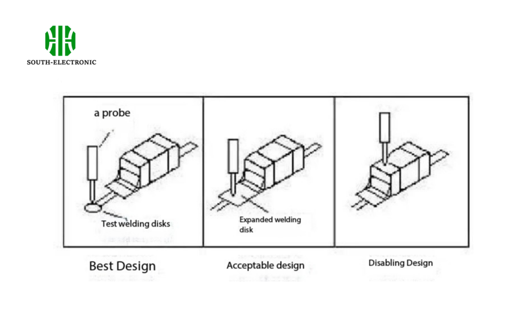
The figure below shows an example of test point design. By extending the wire to set the test pad near the lead of the component or using the via pad to test the node, the test node is strictly prohibited from being selected on the solder joint of the component. This test may cause the cold solder node to be squeezed to the ideal position under the pressure of the probe, so that the cold solder fault is covered up, resulting in the so-called "fault masking effect". Due to the deflection of the probe caused by the positioning error, the probe may directly act on the end point or pin of the component and cause damage to the component.
Conclusion
PCB manufacturability, particularly for electronic assembly, is a pivotal link between design intent and reliable production. Every choice—from assembly method selection and component orientation to clamping edges, positioning marks, and test point placement—directly impacts efficiency, cost, and quality. Designers must embed manufacturability into the core of their process, not as an afterthought. Aligning layouts with assembly constraints (e.g., wave soldering directionality, paneling for small boards), ensuring clear silk-screen correspondence, and prioritizing test point accessibility are non-negotiable for seamless production. In an era of miniaturization, balancing innovation with practical assembly feasibility is key to competitive products.
For expertise that bridges design excellence and manufacturing reality, partner with South-Electronic. Our decades of experience in PCB engineering ensure your designs translate into efficient, high-quality production—every time.

