
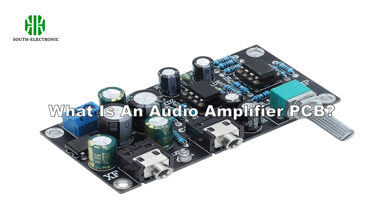
Your phone’s weak bass. Crackling speakers. Muffled vocals. We’ve all suffered from poor sound quality. The audio amplifier PCB[^1] silently solves these frustrations through precise engineering – but how does this unassuming board transform lifeless electrical signals into vibrant music?
An audio amplifier PCB is a specialized circuit board designed to boost weak audio signals while maintaining fidelity. It uses transistors, resistors, capacitors, and inductors arranged with precision to amplify sound without distortion or noise interference, making it essential in speakers, car audio systems, and home theaters.
)
While this definition covers basics, the real magic lies in how these boards achieve crystal-clear amplification. Let’s analyze four critical aspects that make professional-grade audio amplification possible through PCB design.
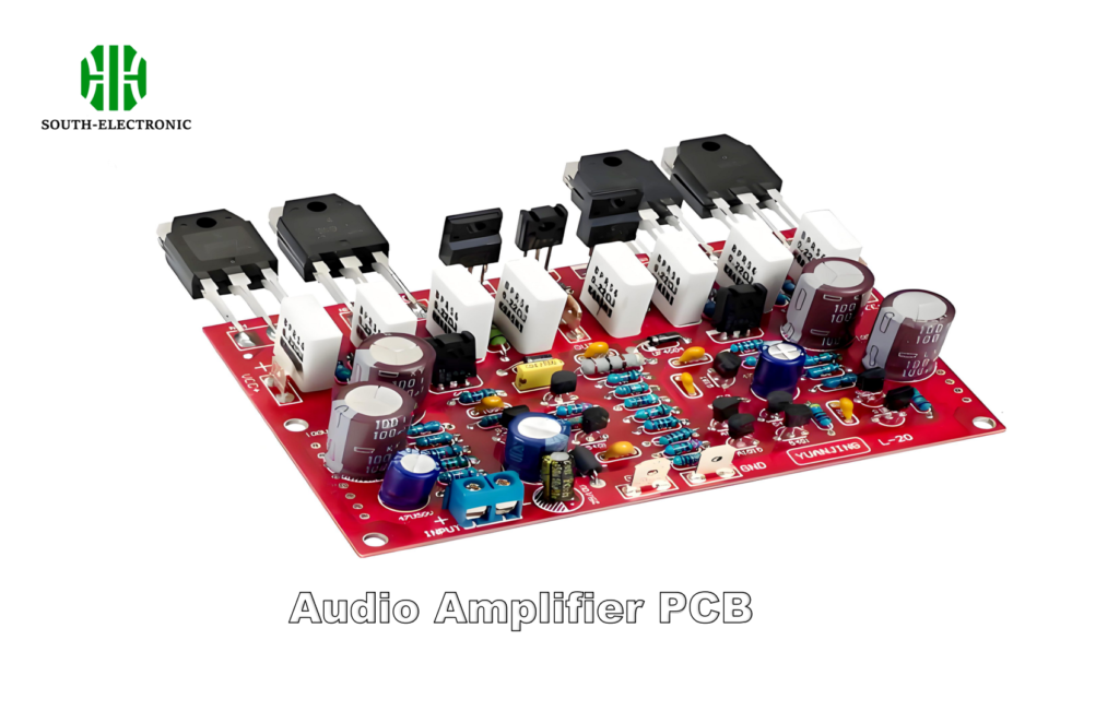
Core Components of an Audio Amplifier PCB
Imagine soldering components blindly. Crackling noise. Signal loss. Every amplifier PCB fails without its essential parts working in harmony. What elements make these boards amplify sound successfully?
Key components include transistors[^2] (signal amplification), resistors (current control), capacitors (signal filtering), inductors (noise reduction), and copper traces (signal routing). These elements work together to accurately boost audio signals across frequency ranges while preventing interference.
)
Component Synergy in Action[^3]
Three critical partnerships define functional amplifier PCBs:
| Component Pair | Role | Performance Impact |
|---|---|---|
| Transistor + Heat Sink | Signal amplification with thermal management | Prevents overheating distortion |
| Capacitor + Inductor | High/Low frequency filtering | Reduces hiss and hum noises |
| Resistors + PCB Traces | Impedance matching | Minimizes signal reflection losses |
The power supply stability directly affects transistor performance – fluctuations cause audible "buzzing." Engineers use parallel capacitors (100μF bulk + 0.1μF decoupling) to filter power line noise. Board material matters too: FR-4 substrates handle home audio, while RF-friendly PTFE laminates better suit high-end studio equipment.
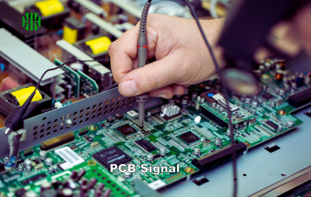
How Audio Amplifier PCBs Enhance Signal Quality
Harsh treble. Weak mids. Boomy bass. Raw audio signals are unbalanced and noisy. How do amplifier boards transform them into rich, distortion-free output?
Quality PCBs improve signals through four stages: input buffering (impedance matching), voltage amplification (signal strengthening), current boosting (power handling), and output filtering (noise removal). Each stage uses specific components arranged to preserve audio details.
)
Noise Suppression Techniques[^4]
Modern boards implement three noise-control strategies:
-
- Entire PCB layer as ground reference
- Reduces electromagnetic interference by 60%
- Lowers crosstalk between components
-
Star Point Grounding
- All grounds meet at central point
- Prevents ground loop hums
- Essential in multi-stage amplifiers
-
Shielded Trace Routing
- Critical paths away from power lines
- Uses guard rings around sensitive traces
- Maintains >80dB signal-to-noise ratio
Differential signal pairing (balanced lines) combined with ground isolation cuts common-mode noise by 45dB. Thermal relief pads prevent solder cracks during heating cycles, ensuring stable connections over years of use.
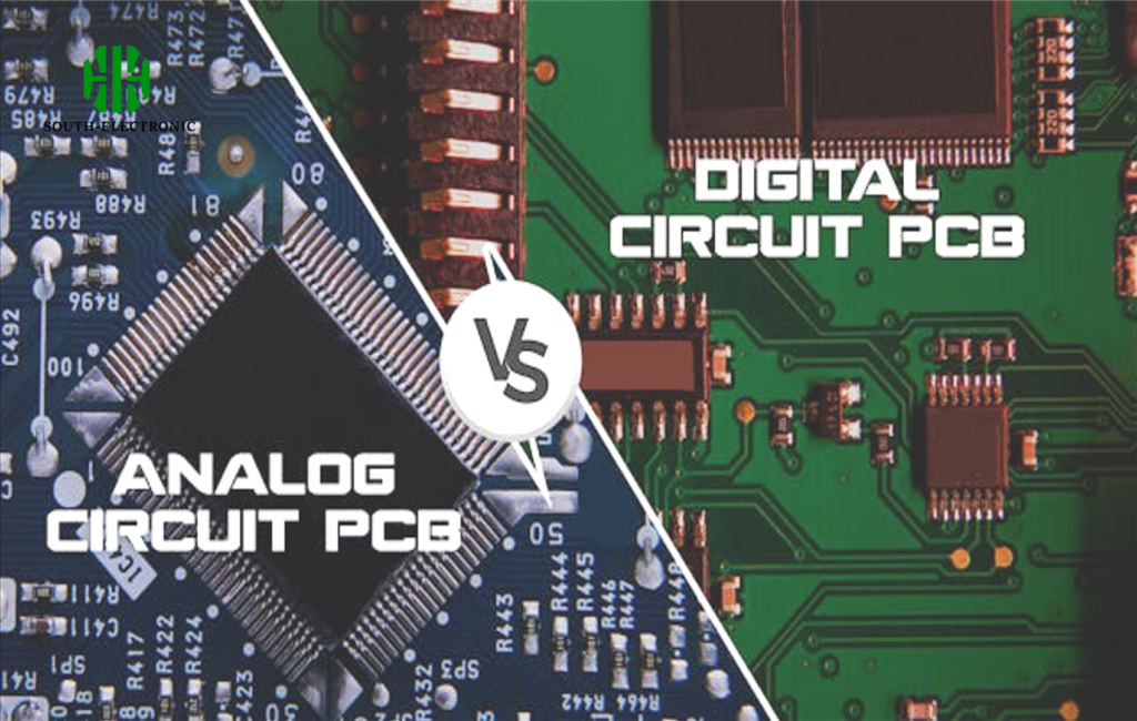
Key Differences Between Analog and Digital Amplifier PCBs
Hissing analog vs. cold digital sound. The eternal debate starts at PCB design level. What separates these two amplifier types physically and functionally?
Analog boards use continuous signal processing with linear components, while digital designs incorporate microcontrollers, DSP chips, and PWM stages. Their layouts, components, and noise profiles differ substantially.
)
Technical Comparison Matrix
| Parameter | Analog PCB | Digital PCB |
|---|---|---|
| Core Components | Op-amps, transistors | MCU, PWM controllers |
| Signal Type | Continuous waveform | Pulse-width modulated |
| Distortion | Harmonic at 0.01% THD | Quantization noise |
| Power Efficiency | 30-50% | 85-95% |
| Layout Priority | Short analog signal paths | Clock signal isolation |
| Component Count | Low (30-50) | High (100+) due to ICs |
| Repair Complexity | Easy component replacement | Requires SMD rework station |
Digital boards demand strict signal integrity – a 100MHz clock needs controlled impedance traces (50Ω ±10%). RF-grade materials like Isola IS410 manage high-speed signals better than standard FR4. Both types require careful thermal design but face different challenges: analog ICs need stable temps for bias stability, while digital chips generate spot heat needing localized cooling.
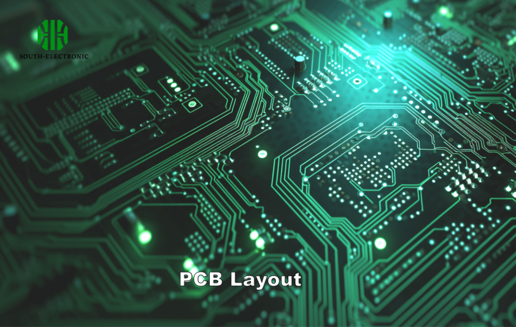
Critical Layout Considerations for Audio Amplifier PCBs
Oscillating outputs. Thermal runaway. RF interference. 90% of amplifier failures trace back to poor PCB layout[^6] choices. What design rules prevent these disasters?
Prioritize component placement sequence: input stage → voltage amp → driver → output transistors → power supply. Maintain star grounding, minimize trace lengths for high-current paths, and implement thermal relief for heat-sensitive parts.
)
Layout Optimization Checklist
-
Power Supply Routing
- Use separate paths for analog/digital grounds
- Place decoupling caps within 5mm of ICs
- 45° bends prevent EMI radiation at corners
-
Signal Flow Management
- Input traces ≤25mm length
- No parallel high/low level traces
- Guard rings around microphone inputs
-
Thermal Design
- Copper pours under power transistors
- 2oz copper thickness for >3A currents
- Thermal vias to inner ground planes
For class-D amplifiers, keep PWM outputs away from analog sections – even 5mm separation reduces crosstalk by 12dB. Multi-layer boards (≥4 layers) allow dedicated power and ground planes. Testing shows 1.6mm board thickness with TG170 material withstands prolonged thermal stress in automotive amplifiers.
Conclusion
Audio amplifier PCBs transform fragile signals into vivid soundscapes through engineered component synergy, intelligent layouts, and precise noise control – the silent architects of our audio experiences.
[^1]: Explore this link to understand the intricate workings of audio amplifier PCBs and their role in enhancing sound quality.
[^2]: Discover the essential components of audio amplifier PCBs and how they contribute to superior sound amplification.
[^3]: Learn about the synergy between components in audio amplifier PCBs and its impact on audio quality and performance.
[^4]: Explore advanced noise suppression techniques to enhance audio quality in amplifier PCBs, ensuring clearer sound and reduced interference.
[^5]: Learn how ground plane design can significantly reduce interference and enhance the performance of audio amplifier PCBs.
[^6]: Understanding PCB layout best practices can significantly enhance the performance and reliability of audio amplifiers.

