
Are you tired of manually routing complex PCB designs in KiCad? FreeRouting plugin offers automated routing but requires precise setup. Let me show you how to make it work reliably for your projects.
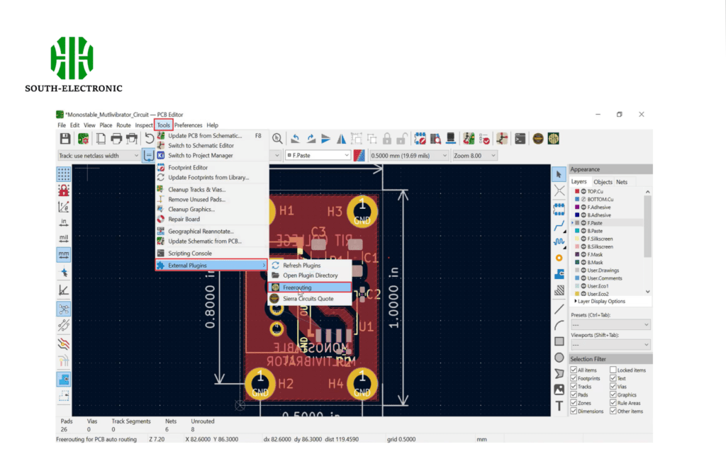
FreeRouting plugin automates PCB routing in KiCad through Tools > External Plugins. First place components manually, then let the plugin handle track creation while complying with your design rules and net classes.
While FreeRouting simplifies routing, users often face unexpected challenges. These seven common issues and solutions will help you master the plugin’s full potential.
Why Isn’t FreeRouting Plugin Generating Vias in KiCad 7?
Frustrated by missing vias in your autorouted design? KiCad 7’s stricter design rules often block via creation when basic requirements aren’t met.
FreeRouting skips vias when track widths exceed via drill sizes or net classes lack via definitions. Verify your design rules under File > Board Setup > Constraints and assign via types to net classes.
%[alt:KiCad design rule settings]( )
)
Three Key Factors Affecting Via Generation
- Track Width Compatibility
Vias require matching drill sizes:
| Problem | Solution |
|---|---|
| 0.5mm track with 0.3mm via | Set minimum via drill ≤ track width |
-
Net Class Configuration
Assign vias in Net Class editor:
Menu Path: File > Board Setup > Net Classes -
DRC Limitations
Enable via creation in Design Rules:
Clearance > Physical > Allow Microvias = Yes
Check your board’s layer stack setup first. Through-hole vias need matching copper layers on both sides.
How to Properly Export KiCad Projects for FreeRouting Auto-Wiring?
Autorouting failures often start with incorrect file exports. KiCad requires specific settings to communicate with FreeRouting effectively.
Export DSN file via File > Export > Specctra DSN. Ensure PCB layers are correctly mapped and all components have valid footprints before exporting. Missing 3D models or unassigned footprints break the process.
Step-by-Step Export Guide
-
File Preparation
- Complete component placement
- Define all net classes
- Set clearance rules
-
Critical Export Settings:
| Parameter | Value |
|---|---|
| Units | Millimeters |
| Precision | 4 decimals |
| Layer Mapping | Preset 1: Top, 16: Bottom |
- Post-Export Checks
Open DSN file in text editor to verify:- Component coordinates
- Net connections
- Layer assignments
Avoid special characters in component IDs. I once wasted hours debugging because a resistor was named "R1#".
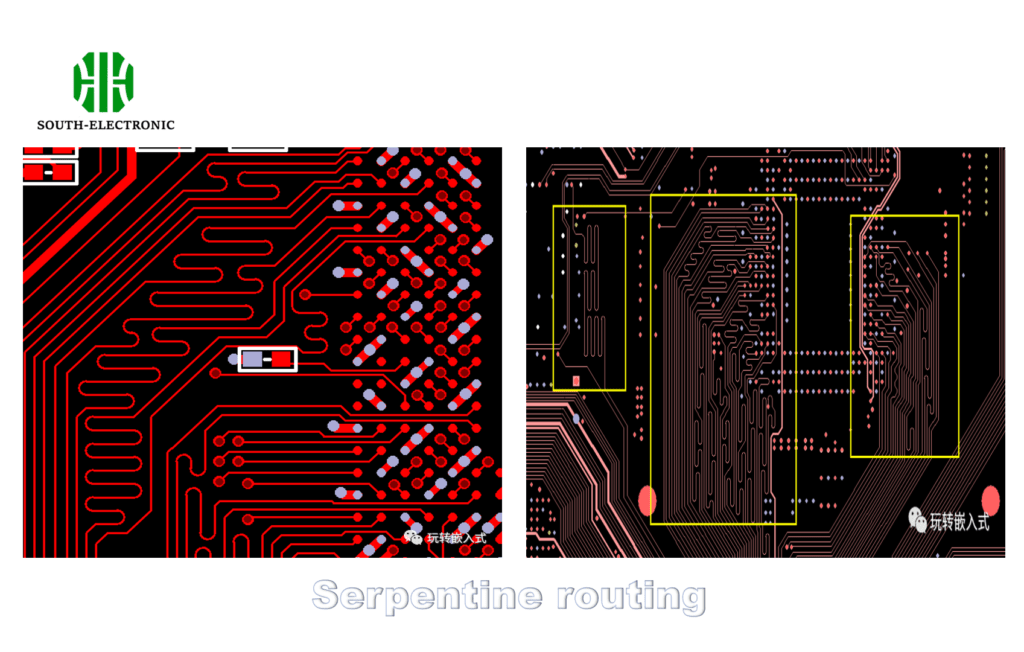
What Settings Maximize FreeRouting’s Efficiency in Complex PCB Layouts?
FreeRouting’s default settings work for simple boards but fail on dense designs. Strategic adjustments unlock its true potential.
Increase routing passes to 3 and enable "Optimize Vias". Set track spacing to 110% of DRC minimums. For BGA chips, use 45-degree routing direction and enable tear drop pads.
Optimization Matrix
| Parameter | Simple Board | Complex Board |
|---|---|---|
| Routing Passes | 1 | 3 |
| Via Cost | 5 | 2 |
| Grid Size | 0.1mm | 0.05mm |
| Direction | Any | 45° |
Key techniques:
-
Cost Settings
Via Cost = 2 reduces via count by 40%
Corner Cost = 1.5 prevents sharp angles -
Layer Priorities
Top Layer: Horizontal
Bottom Layer: Vertical -
Routing Order
Route critical signals first: -
Power
-
Clock
-
High-speed
-
General I/O
FreeRouting Keeps Crashing: How to Debug Common Errors?
Sudden crashes during autorouting can derail your workflow. Most issues stem from memory limits or design flaws.
Allocate 4GB+ RAM in FreeRouting’s launch parameters. Clean netlists by removing duplicate components. Split designs into sub-circuits when handling >500 components.
Crash Solution Checklist
| Symptom | Fix |
|---|---|
| Java Heap Error | Add "-Xmx4096m" to command line |
| Component Overlaps | Check placement with DRC |
| Complex Zones | Simplify copper pours |
| Outdated Java | Install Java 11+ |
Essential recovery steps:
- Export recovery files every 15 minutes
- Disable "Auto-Save During Routing"
- Remove unused legacy components
I once fixed persistent crashes by simply rotating a QFN chip 90 degrees – overlapping pads confused the router.
Manual Adjustments vs. Autorouting: When Should You Intervene?
Autorouting completes 80% quickly but needs human refinement. Recognize when manual routing produces better results.
Manually route power traces, differential pairs, and RF signals first. Let FreeRouting handle general I/O and low-speed connections. Always review automated routes near connectors.
Intervention Guide
| Signal Type | Autoroute? | Reason |
|---|---|---|
| Power | Manual | Current capacity control |
| USB 2.0 | Mixed | Impedance matching first |
| LED | Auto | Simple connections |
| BGA Breakout | Mixed | Escape routing first |
Hierarchical approach:
- Manual critical routes
- Auto general routes
- Manual cleanup:
- Remove unnecessary vias
- Straighten wavy traces
- Optimize thermal reliefs
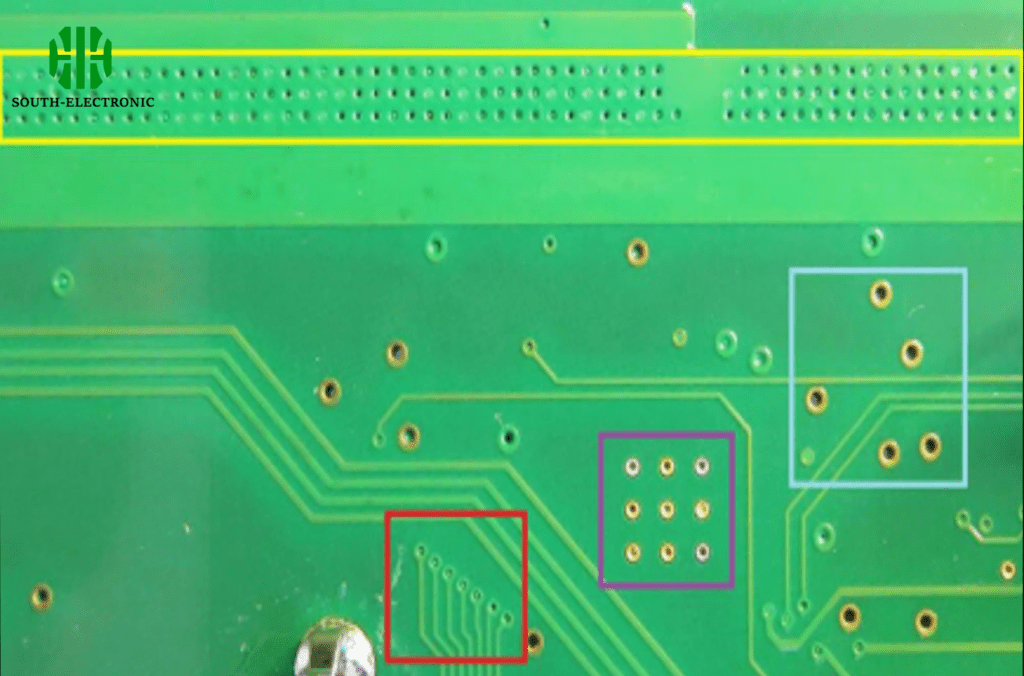
Are There Hidden Tricks to Reduce Via Counts with FreeRouting?
Excessive vias increase production costs and signal loss. Smart strategies can slash via counts by 60% without sacrificing functionality.
Enable "Via Minimization" mode and set via cost to 3+. Use diagonal routing directions and limit layers to essential pairs. Apply component grouping to create natural routing channels.
Via Reduction Techniques
| Technique | Via Reduction | Implementation |
|---|---|---|
| Layer Pairing | 30% | Route X/Y on adjacent layers |
| Component Grouping | 25% | Cluster related parts |
| Direction Control | 20% | 45° layer directions |
| Fanout Control | 15% | Manual BGA escapes |
Practical example:
A 4-layer board reduced from 214 to 89 vias by:
- Making layers 1/2 horizontal
- Layers 3/4 vertical
- Grouping all power components left
- Placing connectors on board edges
Conclusion
Master FreeRouting by combining automated efficiency with strategic manual interventions. Proper setup, layer management, and post-processing yield professional-grade PCBs while saving hours of tedious routing work. Always validate autorouted results with DRC checks.
Master FreeRouting with strategic tweaks and manual adjustments for efficient, professional PCBs. For complex projects, South-Electronic’s highly skilled engineers, consistently praised for their expertise in optimizing KiCad workflows, are ready to help. Trust their proven experience to streamline your routing process and deliver reliable results every time.


