
PCB Design
South-Electronic
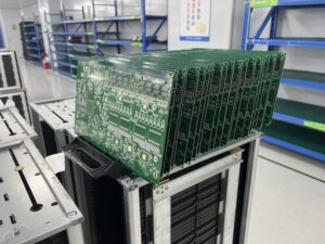
Find greatness in PCB design with South-Electronic, your trusted partner for top-quality, reliable, and cost-effective circuit boards. Whether you need single-layer or multi-layer designs, our customizable solutions meet all your electronic needs, ensuring precision and performance across a range of applications.
Transform Your Projects with Superior PCB!
Welcome to South-Electronic, where you’ll find top-notch Basic PCB Design known for their accuracy and versatility. Our Basic PCB deliver outstanding performance, making them perfect for a wide range of applications. Choose from options like single-layer and multi-layer boards, all customized to meet your specific electronic needs.
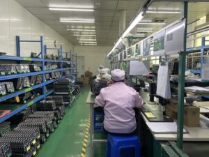
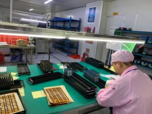
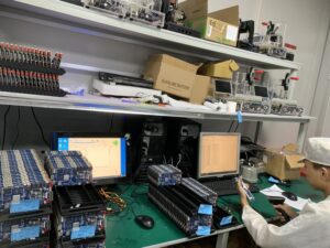
Rely on South-Electronic for unmatched quality and consistency in your electronic projects. Our basic PCBs elevate the performance of your devices through exceptional design and quality. Choose South-Electronic for your next project and experience unparalleled service and superior PCB designs. Get started now for excellence that sets you apart!
Why Choose South-Electronic?
-
Flexibility in Ordering
Order exactly what you need, when you need it.
Whether you're looking for a single prototype or multiple iterations, we tailor every order to meet your unique requirements, ensuring a flexible and smooth process for you. -
Experienced Team
Tap into industry expertise for your next project.
With over a decade of experience, our team is here to help you achieve success with the insights and knowledge we've gained from working across the industry. -
Guartneed Quality
Enjoy the best quality, straight from the manufacturer.
As your primary manufacturer, we guarantee top-notch quality that exceeds what you'll find from other suppliers, giving you the peace of mind you deserve. -
Fast Delivery
Get your orders fast with our efficient production processes.
We understand that time matters. Our streamlined operations ensure you receive your products quickly, keeping your projects on track without delay. -
Guaranteed Satisfaction
All-in-one PCB solutions designed for your satisfaction.
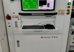
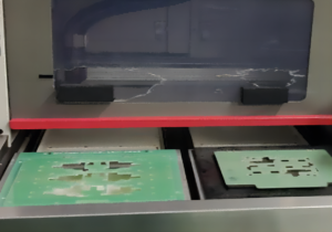
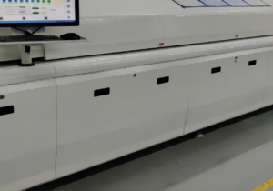
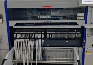
With our extensive range of processing equipment, we provide comprehensive services to meet all your PCB needs, ensuring a seamless experience from start to finish. -
Strategic Supply Chain Efficiency
Your satisfaction is enhanced by our transparency.
Our optimized supply chain processes include real-time tracking and dedicated customer service, improving overall customer satisfaction and operational transparency.
Related Project We had Done
Customer Reviews
Common Questions
Most Popular Questions
Send us a message
The more detailed you fill out, the faster we can move to the next step.


The Complete Guide for Basic PCB Design
Contents
Chapter 1
Introduction to Basic PCB Design
Overview of PCB (Printed Circuit Board)
Have you ever wondered what makes your electronic devices function so smoothly? The answer often lies in the heart of these devices: the Printed Circuit Board (PCB). A PCB is a flat board that mechanically supports and electrically connects electronic components using conductive pathways, tracks, or signal traces etched from copper sheets laminated onto a non-conductive substrate. By understanding PCBs, you unlock the secret to creating reliable and efficient electronic products.
Importance of PCB in Electronic Devices
Why are PCBs so crucial in electronics? Imagine trying to connect all the components of your smartphone, computer, or even a simple remote control without a PCB. It would be a tangled mess of wires, prone to errors and failures. PCBs provide a compact, organized way to connect components, ensuring your devices work seamlessly. They also enhance reliability, making sure that every signal reaches its destination without interference. With a well-designed PCB, you can create products that are not only functional but also durable and efficient.
Basic PCB vs. Advanced PCB: Understanding the Differences
When it comes to PCBs, not all are created equal. Basic PCBs typically involve simpler designs with fewer layers and straightforward routing. They are perfect for less complex applications, where functionality is key but advanced features are not necessary.
On the other hand, advanced PCBs take things to the next level. They often include multiple layers, intricate designs, and support for high-speed signals and complex circuitry. If your project involves sophisticated electronic systems, like high-performance computing or advanced telecommunications, an advanced PCB is what you need.
Understanding these differences helps you make informed decisions about which type of PCB is right for your project. Whether you’re aiming for a simple gadget or a cutting-edge device, choosing the appropriate PCB is crucial for success.
Chapter 2
Understanding PCB Materials
Types of PCB Materials
When you dive into PCB design, one of the first things you’ll encounter is the variety of materials used. Each type of PCB material offers distinct properties that can significantly impact your project’s performance. The most common materials you’ll come across include:
- FR-4: The industry standard for most PCBs, made from woven fiberglass cloth with an epoxy resin binder that is flame resistant.
- Polyimide: Known for its excellent thermal stability, used in flexible and high-temperature applications.
- PTFE (Teflon): Offers superior electrical properties, ideal for high-frequency applications.
- Metal Core: Used for applications that require excellent heat dissipation, like LED lighting and power supplies.
By understanding these materials, you can make informed choices that suit your specific project needs.
Characteristics of FR-4 and Other Common Materials
You’re probably wondering what makes each material unique. Let’s break down the key characteristics of these common PCB materials:
- FR-4:
- Thermal Stability: Can withstand high temperatures without degrading.
- Mechanical Strength: Provides robust support for components.
- Cost-Effective: Widely available and affordable, making it a popular choice.
- Polyimide:
- High Heat Resistance: Performs well in high-temperature environments.
- Flexibility: Ideal for flexible circuits and dynamic applications.
- Durability: Resistant to chemical and mechanical stress.
- PTFE (Teflon):
- Low Dielectric Constant: Ensures minimal signal loss, perfect for high-frequency circuits.
- Heat Resistant: Handles high temperatures with ease.
- Chemical Resistance: Unaffected by most chemicals, making it durable and long-lasting.
- Metal Core:
- Heat Dissipation: Excellent for applications where heat management is critical.
- Stability: Provides a stable base for high-power components.
- Durability: Withstands harsh environmental conditions.
By recognizing these characteristics, you’ll be better equipped to choose the right material for your design.
Selecting the Right Material for Your Project
Choosing the right PCB material is crucial for your project’s success. Here’s how you can make the best choice:
Assess Your Requirements: Consider the electrical, thermal, and mechanical needs of your project. Are you designing a high-frequency circuit? Do you need the PCB to withstand high temperatures? Understanding your project’s specific requirements is the first step.
Match Material Properties: Once you know your needs, match them with the properties of available materials. For example, if you need thermal stability and mechanical strength, FR-4 might be your best bet. For high-frequency applications, PTFE would be more suitable.
Consider Cost: Budget constraints are always a factor. While advanced materials offer superior properties, they also come at a higher cost. Balance your need for performance with your budget to find the best fit.
Prototype and Test: Sometimes, the best way to determine the right material is to prototype and test. Create a small batch of PCBs using different materials and test them under real-world conditions. This approach helps you see how each material performs in your specific application.
By following these steps, you’ll ensure you select the right material for your PCB, leading to a successful and reliable design.
Chapter 3
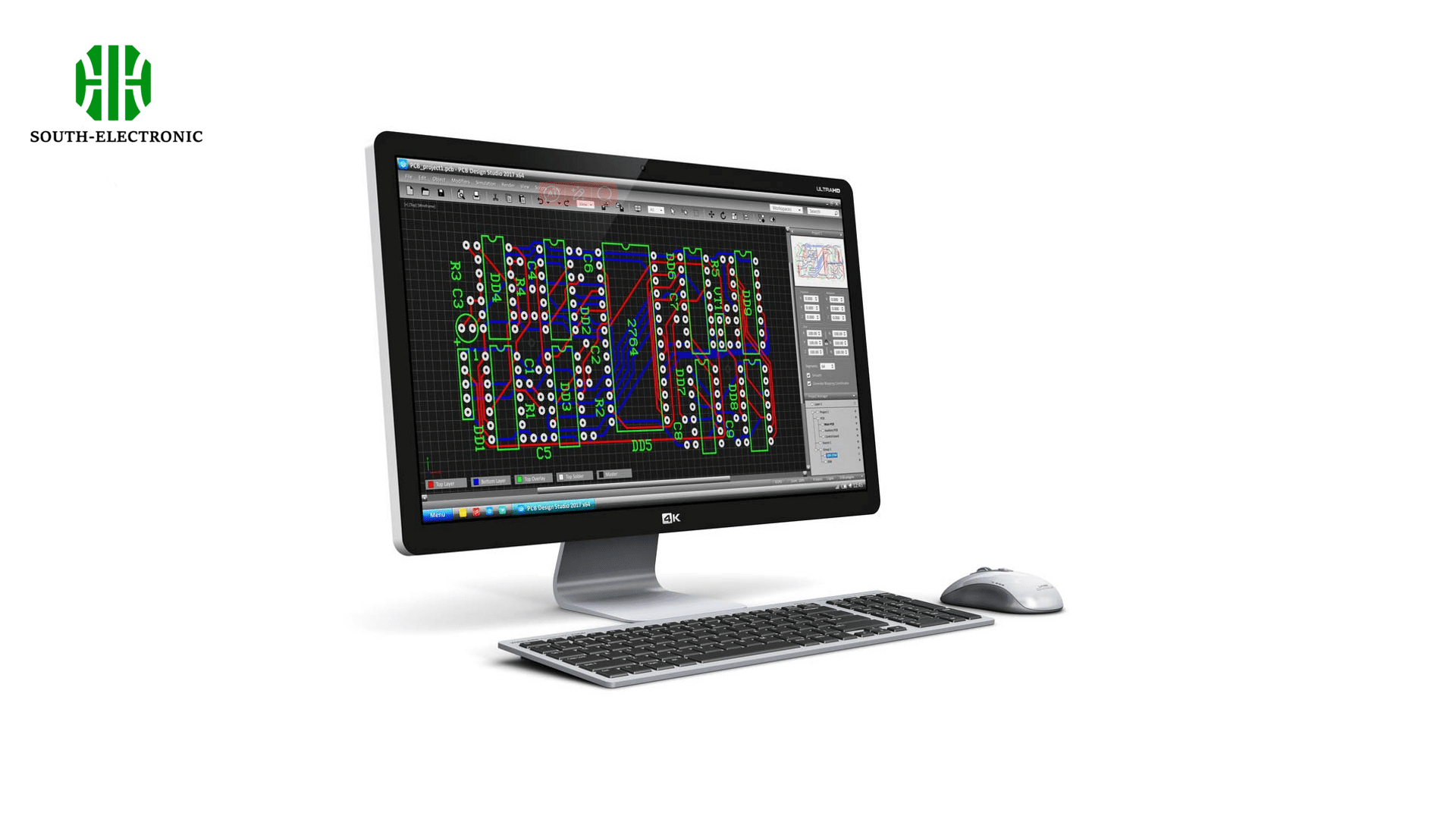
PCB Design Software
Popular PCB Design Software Tools
When you’re ready to start designing your PCB, the right software can make all the difference. Here are some of the most popular PCB design software tools that you can consider:
- Altium Designer: Known for its robust features and user-friendly interface, it’s a favorite among professionals.
- Eagle: A powerful and versatile tool that’s great for both beginners and advanced users.
- KiCad: An open-source option that offers a comprehensive suite of design tools.
- OrCAD: Known for its advanced simulation capabilities and extensive component libraries.
- EasyEDA: A web-based tool that’s easy to use and ideal for quick designs and collaboration.
These tools vary in complexity and features, catering to different needs and levels of expertise.
Features and Benefits of Each Tool
Let’s delve into the features and benefits of each PCB design software to help you understand what makes them stand out:
Altium Designer:
- Integrated Environment: Combines schematic capture, PCB layout, and design documentation in one platform.
- Advanced Routing: Offers powerful routing tools, including interactive routing and auto-routing.
- 3D Visualization: Allows you to view and edit your PCB design in 3D, ensuring precise component placement.
- Extensive Libraries: Provides access to a vast library of components, saving you time in design.
Eagle:
- User-Friendly Interface: Intuitive and easy to navigate, making it great for beginners.
- Component Libraries: Extensive libraries with a wide range of components.
- Scripting Capability: Supports scripts for automating repetitive tasks, boosting productivity.
- Affordable Pricing: Offers a free version for hobbyists and affordable licenses for professionals.
KiCad:
- Open Source: Free to use and supported by a large community of developers.
- Comprehensive Tools: Includes schematic capture, PCB layout, 3D viewer, and more.
- Flexible and Customizable: Allows you to create custom components and footprints.
- Regular Updates: Continuously improved with regular updates and new features.
OrCAD:
- Advanced Simulation: Excellent simulation tools for analyzing and validating your designs.
- High-Performance Routing: Optimized for complex designs with high-speed and high-density requirements.
- Extensive Libraries: Large libraries of pre-built components and models.
- Scalability: Suitable for small projects and large, complex designs alike.
EasyEDA:
- Web-Based: No installation required, accessible from any device with an internet connection.
- Collaboration: Easy sharing and collaboration with team members.
- Integrated Tools: Includes schematic capture, PCB layout, and simulation tools.
- Community Support: Active community and access to shared projects and components.
How to Choose the Best Software for Your Needs
Selecting the best PCB design software depends on your specific requirements and preferences. Here are some tips to help you make the right choice:
Assess Your Skill Level:
- Beginner: If you’re new to PCB design, start with user-friendly tools like Eagle or EasyEDA. They offer intuitive interfaces and helpful tutorials.
- Intermediate/Advanced: For more complex designs, consider Altium Designer, OrCAD, or KiCad. These tools provide advanced features and greater flexibility.
Evaluate Your Project Needs:
- Simple Designs: For straightforward projects, a basic tool like EasyEDA or Eagle might suffice.
- Complex Designs: For high-speed, high-density, or multi-layer PCBs, opt for Altium Designer, OrCAD, or KiCad, which offer powerful routing and simulation capabilities.
Consider Your Budget:
- Free/Open Source: If budget is a concern, KiCad is a great open-source option with robust features.
- Professional Use: For professional and commercial use, investing in a comprehensive tool like Altium Designer or OrCAD can be worthwhile.
Look for Community and Support:
- Community Support: Tools like KiCad and EasyEDA have active communities that can be invaluable for troubleshooting and advice.
- Official Support: Professional tools like Altium Designer and OrCAD offer official support and extensive documentation.
Test and Trial:
- Trial Versions: Many software providers offer free trials. Take advantage of these to test different tools and see which one fits your workflow best.
- Hands-On Experience: Spend some time using the software to understand its interface, features, and how well it integrates with your design process.
By carefully considering these factors, you can choose the PCB design software that best meets your needs, enhancing your design efficiency and project success.
Chapter 4
Designing Your First PCB
Step-by-Step Guide to Creating a Basic PCB Layout
Are you ready to design your first PCB? Follow these steps to create a basic PCB layout that meets your project’s needs.
Define Your Requirements:
- List Components: Identify all the components you need for your project.
- Schematic Diagram: Draw a schematic diagram to map out how each component connects.
Choose Your PCB Design Software:
- Select a user-friendly software tool such as Eagle or KiCad to start your design process.
Create the Schematic:
- Place Components: Use the software to place each component on your schematic.
- Connect Components: Draw lines to connect the components as per your circuit design.
Design the PCB Layout:
- Component Placement: Arrange the components on the PCB layout, ensuring an optimal layout for signal flow and space utilization.
- Routing: Connect the components using copper traces, paying attention to trace width and spacing to ensure proper electrical performance.
- Add Vias: If you’re using a multi-layer PCB, add vias to connect traces between layers.
Generate the Gerber Files:
- Check Design: Use the software’s design rule check (DRC) to identify and fix any errors.
- Export Files: Once your design is complete, export the Gerber files, which are used by manufacturers to produce your PCB.
Review and Prototype:
- Review: Double-check your design and Gerber files for any errors.
- Prototype: Send your design to a PCB manufacturer to create a prototype.
Key Considerations for Beginners
Starting with PCB design can be exciting and a bit challenging. Here are some key considerations to keep in mind:
Component Placement:
- Place components logically, keeping related parts close together.
- Ensure components are oriented correctly for easy soldering and assembly.
Trace Width and Spacing:
- Use appropriate trace widths for the current they will carry.
- Maintain proper spacing between traces to avoid short circuits and interference.
Power and Ground Planes:
- Use dedicated planes for power and ground to reduce noise and improve signal integrity.
Thermal Management:
- Consider thermal relief for components that generate heat.
- Use thermal vias and copper pours to dissipate heat efficiently.
Design Rules:
- Follow design rules specified by your PCB manufacturer to ensure your design can be produced accurately.
Common Mistakes to Avoid
Avoiding common pitfalls will save you time and frustration. Here are some mistakes to watch out for:
Poor Component Placement:
- Don’t place components too close to each other, which can make soldering difficult and increase the risk of shorts.
Incorrect Trace Widths:
- Avoid using trace widths that are too narrow for the current they need to carry, which can cause overheating and failure.
Ignoring Design Rules:
- Don’t ignore the design rules provided by your manufacturer. Violating these rules can lead to production errors and increased costs.
Lack of Testing:
- Don’t skip the prototype stage. Testing your design with a prototype helps catch errors before full-scale production.
Inadequate Documentation:
- Make sure to document your design process and decisions thoroughly. This will help you and others understand the design later on.
Overcomplicating the Design:
- Keep your design as simple as possible, especially when you’re just starting. Complexity can lead to more errors and difficulties in troubleshooting.
By following these steps, keeping key considerations in mind, and avoiding common mistakes, you’ll be well on your way to designing your first successful PCB. Let’s continue exploring more about PCB design to enhance your skills and project outcomes.
Chapter 5
PCB Schematic Design
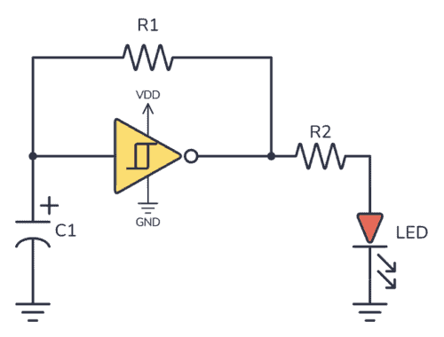
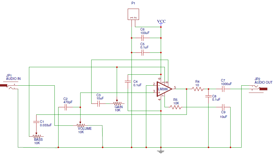
What is a PCB Schematic?
Have you ever wondered how electronic components connect to create a functional circuit? That’s where a PCB schematic comes in. A PCB schematic is a graphical representation of your electronic circuit. It shows how components like resistors, capacitors, and ICs (integrated circuits) connect using lines that represent electrical connections. Think of it as the blueprint for your PCB layout, guiding the placement and routing of your components on the actual board.
Creating and Reading PCB Schematics
Creating and reading PCB schematics is an essential skill for any electronics project. Here’s how you can get started:
Start with a Clear Plan:
- Identify Components: List all the components you need for your circuit.
- Understand Connections: Know how each component should connect with others.
Use Schematic Design Software:
- Choose Your Tool: Select a user-friendly schematic design software like Eagle, KiCad, or Altium Designer.
- Place Components: Drag and drop symbols for each component onto your schematic workspace.
- Draw Connections: Use lines to connect the components as per your circuit plan. These lines represent the electrical connections or nets.
Label and Organize:
- Component Labels: Assign reference designators (e.g., R1, C1, U1) to each component for easy identification.
- Net Labels: Label important nets, such as power and ground, for clarity.
Review and Validate:
- Check Connections: Ensure all connections are correct and complete.
- Run ERC (Electrical Rule Check): Use the software’s built-in ERC tool to identify any potential issues like unconnected pins or short circuits.
Reading a PCB schematic involves understanding the symbols and connections:
- Symbols: Recognize the standardized symbols for different components (e.g., resistors, capacitors, transistors).
- Connections: Follow the lines (nets) to see how components connect and interact.
- Reference Designators: Use the labels to identify and locate specific components.
Tips for Effective Schematic Design
Creating an effective schematic ensures your PCB functions correctly and is easy to understand. Here are some tips to help you design better schematics:
Keep it Organized:
- Logical Layout: Arrange components logically, grouping related components together.
- Clear Paths: Avoid crossing lines to keep the schematic clean and easy to follow.
Label Everything:
- Descriptive Labels: Use clear and descriptive labels for components and nets. This makes troubleshooting and collaboration easier.
- Consistent Naming: Maintain consistency in naming conventions for easy identification.
Use Standard Symbols:
- Standardized Symbols: Stick to industry-standard symbols for components. This ensures anyone reading the schematic can understand it easily.
Document Connections:
- Notes and Annotations: Add notes or annotations to explain complex parts of the circuit.
- Pin Numbers: Clearly label pin numbers on connectors and ICs.
Plan for Test Points:
- Test Points: Include test points in your design for easy debugging and testing. This helps you quickly verify the functionality of your circuit.
Double-Check Connections:
- Visual Inspection: Carefully inspect your schematic to ensure all connections are correct.
- ERC (Electrical Rule Check): Use the ERC tool in your software to identify and fix potential issues.
Simplify Where Possible:
- Minimize Complexity: Keep your design as simple as possible while meeting your requirements. Simpler designs are easier to read and less prone to errors.
Think Ahead:
- Future Modifications: Design with future modifications and expansions in mind. Leave space for additional components or features.
By following these tips, you’ll create clear, accurate, and effective PCB schematics. This foundation will help you design reliable and functional PCBs, bringing your electronic projects to life. Let’s continue exploring more about PCB design to further enhance your skills and project outcomes.
Chapter 6
PCB Layout Design
Principles of Good PCB Layout
Creating a well-designed PCB layout is crucial for the functionality and reliability of your electronic project. Here’s how you can ensure your PCB layout adheres to the best principles:
Clear Component Placement:
- Logical Grouping: Group components logically according to their function. This makes the layout easier to understand and troubleshoot.
- Space Management: Ensure there is enough space between components for heat dissipation and ease of soldering.
Efficient Routing:
- Shortest Path: Keep traces as short and direct as possible to minimize resistance and signal loss.
- Layer Management: Use different layers effectively, with one dedicated to ground planes to reduce noise.
Signal Integrity:
- Ground Planes: Use continuous ground planes to provide a low-impedance path and reduce noise.
- Impedance Matching: Ensure traces carrying high-frequency signals have controlled impedance.
Thermal Management:
- Heat Dissipation: Place heat-generating components away from sensitive ones and use thermal vias to dissipate heat.
Design for Manufacturability:
- Standard Sizes: Stick to standard component sizes and footprints to simplify assembly.
- Clearances: Maintain proper clearances to avoid shorts and ensure reliable operation.
Techniques for Optimal Component Placement
Placing components correctly on your PCB is essential for a functional and efficient design. Here’s how you can achieve optimal component placement:
Prioritize Critical Components:
- Power Supply: Place power supply components first to ensure stable power distribution.
- High-Speed Signals: Position components with high-speed signals to minimize trace lengths and avoid signal integrity issues.
Consider Heat Management:
- Thermal Zones: Group heat-generating components and provide adequate cooling solutions.
- Distance from Sensitive Components: Keep heat-sensitive components away from heat sources.
Follow Signal Flow:
- Logical Flow: Arrange components in the order of signal flow. This makes routing easier and more intuitive.
- Minimize Crosstalk: Place components to minimize the chances of crosstalk between signals.
Accessibility for Testing and Debugging:
- Test Points: Ensure test points and critical components are accessible for probing.
- Component Orientation: Align components uniformly to make manual inspection and testing easier.
Balance Between Layers:
- Layer Distribution: Distribute components evenly across layers to avoid mechanical stress and warping during manufacturing.
Routing Strategies for Signal Integrity
Routing your PCB correctly is vital to maintaining signal integrity and ensuring reliable performance. Here are some key strategies:
Use Ground and Power Planes:
- Dedicated Planes: Utilize dedicated ground and power planes to reduce noise and provide stable reference voltages.
- Short Return Paths: Ensure signal return paths are short and direct by placing ground planes close to signal layers.
Control Trace Impedance:
- Impedance Matching: Match the impedance of high-speed signal traces to prevent signal reflections and ensure signal integrity.
- Consistent Trace Width: Maintain consistent trace width for high-frequency signals to control impedance.
Minimize Crosstalk:
- Trace Spacing: Maintain adequate spacing between parallel signal traces to reduce crosstalk.
- Shielding: Use ground traces or planes between high-speed signal traces to shield them from interference.
Avoid Signal Loop Areas:
- Minimize Loops: Keep signal loops as small as possible to reduce electromagnetic interference (EMI).
- Proper Decoupling: Use decoupling capacitors close to power pins of ICs to filter out noise.
Use Differential Pairs:
- Pair Routing: Route differential pairs (e.g., for high-speed data lines) together with consistent spacing and length to ensure signal integrity.
- Minimize Skew: Ensure equal lengths for differential pairs to prevent skew and maintain signal integrity.
Route Sensitive Signals Carefully:
- Avoid Noisy Areas: Keep sensitive signal traces away from noisy components and traces.
- Filter and Shield: Use filters and shielding for sensitive signals to protect them from noise.
By following these principles and techniques, you’ll create a PCB layout that is efficient, reliable, and optimized for signal integrity. Let’s continue to explore more about PCB design and further enhance your skills to bring your electronic projects to life successfully.
Chapter 7

Manufacturing Process
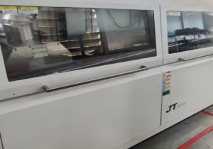
PCB Fabrication Steps
Are you ready to see your PCB design come to life? Understanding the PCB fabrication process is key to ensuring your project’s success. Here’s a step-by-step guide to the PCB fabrication steps:
Design Preparation:
- Generate Gerber Files: Convert your PCB design into Gerber files, which are the standard file format used by PCB manufacturers.
- Design Verification: Double-check your design and run a Design Rule Check (DRC) to catch any potential issues.
Material Selection:
- Choose Substrate: Select the appropriate base material (e.g., FR-4) for your PCB.
- Copper Cladding: Apply a layer of copper to both sides of the substrate.
Image Transfer:
- Photoresist Application: Apply a photoresist layer over the copper-clad board.
- Exposure: Use UV light to transfer your PCB design onto the photoresist layer.
- Development: Develop the exposed board to reveal the copper pattern.
Etching:
- Copper Etching: Remove the unprotected copper using an etching solution, leaving only the desired copper traces.
Drilling:
- Hole Drilling: Drill holes for vias, through-hole components, and mounting points.
Plating:
- Copper Plating: Plate the drilled holes with copper to create electrical connections between layers.
- Surface Finish: Apply a surface finish (e.g., HASL, ENIG) to protect the copper and improve solderability.
Solder Mask and Silkscreen:
- Solder Mask: Apply a solder mask to protect the PCB and prevent solder bridges.
- Silkscreen: Print labels and component designators on the board for easy identification and assembly.
Final Inspection:
- Electrical Testing: Perform electrical tests to ensure all connections are correct.
- Visual Inspection: Inspect the board for any physical defects or issues.
Cutting and Packaging:
- Board Cutting: Cut the PCB into individual units if multiple boards are fabricated on a single panel.
- Packaging: Package the PCBs carefully to prevent damage during shipping.
Understanding PCB Prototyping
Prototyping is a crucial step in the PCB design process. It allows you to test and verify your design before committing to full-scale production. Here’s what you need to know about PCB prototyping:
Why Prototype?
- Design Verification: Prototyping helps you verify that your design works as intended and meets your specifications.
- Identify Issues: Catch and fix any design flaws or errors before mass production, saving time and cost.
- Performance Testing: Test the performance and reliability of your PCB in real-world conditions.
Prototype Types:
- Single-Sided: For simple designs with components on one side only.
- Double-Sided: For more complex designs with components on both sides.
- Multi-Layer: For high-density designs requiring multiple layers.
Prototyping Process:
- Small Batch Production: Manufacturers typically produce a small batch of PCBs for prototyping.
- Testing and Validation: Perform thorough testing to validate the functionality and performance of the prototype.
- Iterate: Make any necessary design adjustments based on testing results and produce additional prototypes if needed.
Choosing a Prototyping Service:
- Speed: Look for a manufacturer that offers quick turnaround times to accelerate your development process.
- Cost: Consider the cost of prototyping services and balance it with your budget.
- Support: Choose a manufacturer that provides good customer support and can assist with any issues during the prototyping phase.
How to Choose a PCB Manufacturer
Selecting the right PCB manufacturer is critical to the success of your project. Here’s how you can make the best choice:
Evaluate Experience and Expertise:
- Industry Experience: Look for manufacturers with a proven track record in PCB fabrication.
- Technical Expertise: Ensure the manufacturer has the technical capabilities to handle your specific requirements.
Check Quality Standards:
- Certifications: Verify that the manufacturer holds relevant certifications (e.g., ISO9001) indicating their commitment to quality.
- Quality Control: Inquire about their quality control processes and testing procedures to ensure high-quality PCBs.
Assess Manufacturing Capabilities:
- Capabilities: Confirm that the manufacturer can produce the type of PCB you need (e.g., single-sided, multi-layer, flexible).
- Equipment: Ensure they use advanced and well-maintained equipment for precise and reliable fabrication.
Review Turnaround Time:
- Lead Times: Check the manufacturer’s lead times for both prototypes and full production runs to ensure they can meet your deadlines.
- Flexibility: Look for flexibility in accommodating urgent or unexpected orders.
Consider Cost:
- Pricing: Compare pricing from multiple manufacturers to find a competitive rate without compromising on quality.
- Value: Consider the overall value, including quality, service, and support, rather than just the lowest price.
Customer Support:
- Communication: Choose a manufacturer with responsive and helpful customer support to address any concerns or issues.
- Assistance: Ensure they offer assistance throughout the process, from design to delivery.
By following these steps and considerations, you’ll be able to choose a PCB manufacturer that meets your needs and ensures the success of your project. Let’s continue to explore more about PCB design to further enhance your skills and bring your electronic projects to life successfully.
Chapter 8
Quality Assurance and Testing
Importance of PCB Testing
Ensuring the quality and reliability of your PCBs is crucial for the success of your electronic projects. Here’s why PCB testing is so important:
- Reliability: You want your devices to perform consistently without failures. Testing helps identify and fix potential issues, ensuring your PCBs work reliably over time.
- Performance: Your goal is to achieve optimal performance from your electronic components. Testing verifies that your PCB meets design specifications and performs as expected.
- Compliance: You need to meet industry standards and regulatory requirements. Testing ensures your PCBs comply with necessary standards, avoiding legal and operational issues.
- Cost Savings: You aim to minimize costly errors and rework. Early testing helps catch problems before mass production, saving you time and money.
- Customer Satisfaction: You want to deliver high-quality products that satisfy your customers. Thorough testing guarantees the quality of your PCBs, leading to happy and loyal customers.
Common Testing Methods
To ensure the quality of your PCBs, various testing methods are employed. Here are some common ones:
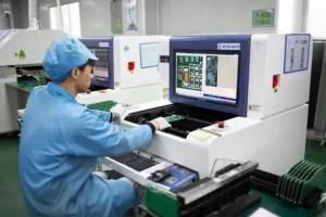
Visual Inspection:
- Purpose: To identify obvious defects such as solder bridges, misaligned components, and visible damage.
- Method: Inspect the PCB visually, often using magnification tools or automated optical inspection (AOI) systems.
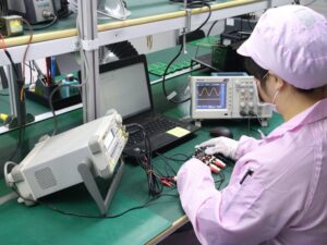
Electrical Testing:
- In-Circuit Testing (ICT):
- Purpose: To check for shorts, opens, resistance, capacitance, and other electrical parameters.
- Method: Use test probes to make electrical contact with test points on the PCB and measure various parameters.
- Flying Probe Testing:
- Purpose: Similar to ICT but used for lower-volume production where test fixtures are not cost-effective.
- Method: Use moving probes to test the PCB without the need for custom fixtures.
- In-Circuit Testing (ICT):
Functional Testing:
- Purpose: To verify the overall functionality of the PCB in real-world conditions.
- Method: Simulate the actual operating environment and test the PCB’s performance in the final product configuration.
Burn-In Testing:
- Purpose: To identify early failures and ensure long-term reliability by stressing the PCB under high temperatures and loads.
- Method: Operate the PCB at elevated temperatures and voltages for an extended period.
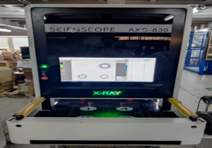
X-Ray Inspection:
- Purpose: To detect hidden defects, such as voids in solder joints or internal layers.
- Method: Use X-ray imaging to examine the internal structure of the PCB without damaging it.
Ensuring Quality in Your PCB Design
To ensure your PCB design maintains high quality, follow these best practices:
Design Rule Checks (DRC):
- Purpose: To catch design errors early.
- Method: Use your design software’s DRC feature to identify issues like spacing violations, unconnected nets, and other design rule breaches.
Component Selection:
- Purpose: To ensure reliable performance.
- Method: Choose high-quality components from reputable suppliers and verify their specifications against your requirements.
Proper Documentation:
- Purpose: To avoid misunderstandings and errors.
- Method: Maintain detailed and clear documentation, including schematics, layouts, bill of materials (BOM), and assembly instructions.
Prototyping and Testing:
- Purpose: To validate your design before mass production.
- Method: Create and test prototypes to identify and fix any issues. Iterate as necessary to refine your design.
Thermal Management:
- Purpose: To prevent overheating and ensure long-term reliability.
- Method: Design with adequate thermal relief, heat sinks, and proper ventilation to manage heat effectively.
Signal Integrity:
- Purpose: To ensure reliable signal transmission.
- Method: Follow best practices for trace routing, such as controlled impedance, proper termination, and minimizing crosstalk.
Regular Audits and Reviews:
- Purpose: To continuously improve quality.
- Method: Conduct regular design reviews and audits to ensure compliance with quality standards and identify areas for improvement.
Manufacturing Collaboration:
- Purpose: To ensure manufacturability and quality.
- Method: Work closely with your PCB manufacturer to understand their capabilities and incorporate their feedback into your design.
By incorporating these testing methods and quality assurance practices, you’ll ensure your PCBs are of the highest quality, leading to reliable and successful electronic products. Let’s continue to explore more about PCB design to enhance your skills and bring your projects to life successfully.

Chapter 9
Cost-Effective PCB Design Strategies
Reducing PCB Design Costs
You want to create high-quality PCBs without breaking the bank. Here’s how you can reduce your PCB design costs effectively:
Simplify Your Design:
- Minimize Layers: Use the fewest number of layers necessary to meet your requirements. Fewer layers mean lower manufacturing costs.
- Standard Components: Stick to standard, widely available components to avoid premium prices.
- Compact Layout: Optimize the layout to fit within smaller board sizes, reducing material costs.
Efficient Use of Materials:
- Panelization: Maximize the use of PCB panels by arranging your design to minimize waste. This increases the number of PCBs you get per panel, lowering the cost per unit.
- Thin Boards: Choose thinner boards if they meet your design requirements, as they often cost less.
Design for Manufacturability (DFM):
- DFM Guidelines: Follow DFM guidelines to avoid complex features that increase manufacturing time and costs.
- Avoid Uncommon Specs: Use common specs for trace width, spacing, and hole sizes to streamline production and reduce costs.
Optimize Component Placement:
- Reduce Assembly Time: Place components to minimize the time and complexity of assembly. This reduces labor costs.
- Automated Assembly: Design for automated assembly to take advantage of cost savings from faster, more accurate machine placement.
Collaborate with Manufacturers:
- Early Involvement: Involve your manufacturer early in the design process to get feedback on cost-saving measures.
- Supplier Discounts: Leverage relationships with suppliers to get bulk discounts on components.
Balancing Quality and Budget
Achieving the right balance between quality and budget is crucial. Here’s how you can strike that balance:
Prioritize Critical Areas:
- Focus on Key Components: Invest in high-quality components for critical areas of your design while using more cost-effective options elsewhere.
- Quality Control: Ensure stringent quality control measures for essential parts of the PCB to maintain overall reliability.
Cost vs. Performance:
- Evaluate Trade-offs: Understand where you can make trade-offs between cost and performance without compromising essential functions.
- Prototype Testing: Conduct thorough prototype testing to identify the minimum viable specifications needed to maintain quality.
Long-Term Savings:
- Durability: Invest in durable materials and reliable components that may cost more upfront but save money in the long run by reducing failures and replacements.
- Energy Efficiency: Design for energy efficiency to lower operating costs over the product’s lifecycle.
Supplier Relationships:
- Negotiate Terms: Build strong relationships with suppliers to negotiate better terms and pricing.
- Consistent Orders: Place consistent, predictable orders to take advantage of volume discounts and preferred pricing.
Tips for Economical PCB Production
Here are some practical tips to make your PCB production more economical:
Batch Production:
- Large Batches: Produce larger batches to reduce the cost per unit. This also helps in negotiating better pricing with manufacturers.
- Combine Orders: If you have multiple projects, combine them into a single production run to share setup costs.
Design for Standard Processes:
- Avoid Custom Features: Stick to standard manufacturing processes and avoid custom features that can increase costs.
- Standard Sizes: Use standard board sizes and shapes to minimize special tooling and setup costs.
Streamline Assembly:
- Surface Mount Technology (SMT): Use SMT components where possible to speed up assembly and reduce labor costs.
- Panel Design: Design PCBs in panels for automated assembly and testing, which lowers production time and costs.
Material Choices:
- Cost-Effective Materials: Choose cost-effective materials that meet your performance requirements without unnecessary expense.
- Alternative Suppliers: Source materials from multiple suppliers to find the best prices and availability.
Testing and Quality Assurance:
- Automated Testing: Implement automated testing to quickly identify and fix defects, reducing the cost of rework.
- Consistent Standards: Maintain consistent quality standards to avoid costly mistakes and ensure reliable production runs.
By implementing these cost-effective PCB design strategies, you’ll be able to reduce expenses while maintaining high quality, ultimately leading to successful and economical electronic products. Let’s continue exploring more about PCB design to further enhance your skills and bring your projects to life efficiently.
Chapter 10
Advanced Tips and Best Practices
Staying Updated with PCB Design Trends
In the fast-paced world of electronics, staying updated with the latest PCB design trends is crucial. Here’s how you can keep up:
Follow Industry News:
- Tech Blogs and Websites: Regularly read tech blogs and industry websites like PCB Design World, Electronics Weekly, and EDN Network to stay informed about new technologies and trends.
- Newsletters: Subscribe to newsletters from leading PCB manufacturers and design software companies to receive updates directly in your inbox.
Join Online Communities:
- Forums and Groups: Participate in forums like PCB Design Forum and LinkedIn groups related to PCB design. Engage in discussions and learn from the experiences of other professionals.
- Social Media: Follow industry experts and companies on social media platforms like Twitter, LinkedIn, and Facebook for real-time updates.
Attend Webinars and Conferences:
- Industry Events: Attend webinars, virtual conferences, and trade shows to learn about the latest advancements and network with other professionals.
- Workshops: Participate in workshops and training sessions to gain hands-on experience with new tools and techniques.
Educational Platforms:
- Online Courses: Enroll in online courses and certifications from platforms like Coursera, Udemy, and LinkedIn Learning to enhance your skills and knowledge.
- Webinars: Participate in webinars hosted by industry leaders and educational institutions to learn about emerging trends and best practices.
Resources for Continuous Learning
Continuous learning is essential for staying ahead in PCB design. Here are some valuable resources to support your growth:
Books and Publications:
- Essential Books: Read foundational books like “The Circuit Designer’s Companion” by Peter Wilson and “PCB Design for Real-World EMI Control” by Bruce R. Archambeault.
- Magazines: Subscribe to industry magazines like PCB007 Magazine and Circuit Cellar for regular insights and articles.
Online Courses:
- Advanced Training: Take advanced courses in PCB design, signal integrity, and EMI/EMC on platforms like IPC EDGE, Altium Academy, and Cadence Training.
- Specialized Topics: Look for courses that cover specialized topics such as high-speed PCB design, RF PCB design, and PCB thermal management.
Technical Blogs and Websites:
- Expert Blogs: Follow technical blogs by industry experts like Eric Bogatin, Rick Hartley, and Dr. Howard Johnson for deep insights and advanced tips.
- Manufacturer Resources: Utilize resources provided by PCB manufacturers and design software companies, including whitepapers, case studies, and application notes.
Community Forums:
- Discussion Platforms: Engage with online communities such as Stack Exchange (Electronics), Reddit (PCB Design), and EEVblog Forum to ask questions, share knowledge, and learn from peers.
- User Groups: Join user groups for specific PCB design software like AltiumLive and KiCad.info to access exclusive content and support.
Expert Tips for Successful PCB Projects
Here are some expert tips to help you achieve success in your PCB design projects:
Early Planning:
- Define Objectives: Clearly define your project objectives, specifications, and constraints before starting the design process.
- Budget and Timeline: Establish a realistic budget and timeline to ensure your project stays on track.
Design for Manufacturability (DFM):
- Simplify Design: Keep your design as simple as possible to reduce manufacturing complexity and costs.
- Standard Practices: Follow industry-standard design rules and guidelines to ensure compatibility with manufacturing processes.
Collaboration and Communication:
- Team Collaboration: Work closely with your team, including engineers, manufacturers, and stakeholders, to ensure everyone is aligned.
- Clear Documentation: Maintain clear and detailed documentation for all aspects of your design, including schematics, layouts, and BOMs.
Prototyping and Testing:
- Iterative Prototyping: Create prototypes and iterate based on testing results to refine your design and catch issues early.
- Comprehensive Testing: Perform thorough testing, including functional, thermal, and EMI/EMC tests, to ensure reliability and performance.
Signal Integrity and EMI/EMC:
- Best Practices: Follow best practices for signal integrity and EMI/EMC, such as controlled impedance, proper grounding, and shielding techniques.
- Simulation Tools: Use simulation tools to predict and mitigate potential signal integrity and EMI issues before physical testing.
Thermal Management:
- Heat Dissipation: Incorporate effective thermal management strategies, such as thermal vias, heat sinks, and copper pours, to prevent overheating.
- Component Placement: Position heat-generating components strategically to optimize airflow and heat dissipation.
Continuous Improvement:
- Learn from Experience: Analyze completed projects to identify areas for improvement and apply those lessons to future designs.
- Stay Curious: Keep exploring new technologies, tools, and techniques to continually enhance your skills and capabilities.
By staying updated with trends, utilizing continuous learning resources, and applying expert tips, you’ll be well-equipped to create successful and innovative PCB designs. Let’s continue to explore more about PCB design to further enhance your skills and bring your projects to life with excellence.
Get in touch
Where Are We?
Industrial Park, No. 438 Donghuan Road, No. 438, Shajing Donghuan Road, Bao'an District, Shenzhen, Guangdong, China
Floor 4, Zhihui Creative Building, No.2005 Xihuan Road, Shajing, Baoan District, Shenzhen, China
ROOM A1-13,FLOOR 3,YEE LIM INDUSTRIAL CENTRE 2-28 KWAI LOK STREET, KWAI CHUNG HK
service@southelectronicpcb.com
Phone : +86 400 878 3488
Send us a message
The more detailed you fill out, the faster we can move to the next step.

