
Modern electronics demand compact designs without sacrificing performance. You’ve seen complex circuit boards, but hidden connections underneath components still puzzle many engineers. Let me explain the key to high-density packaging[^1] that solves these space challenges.
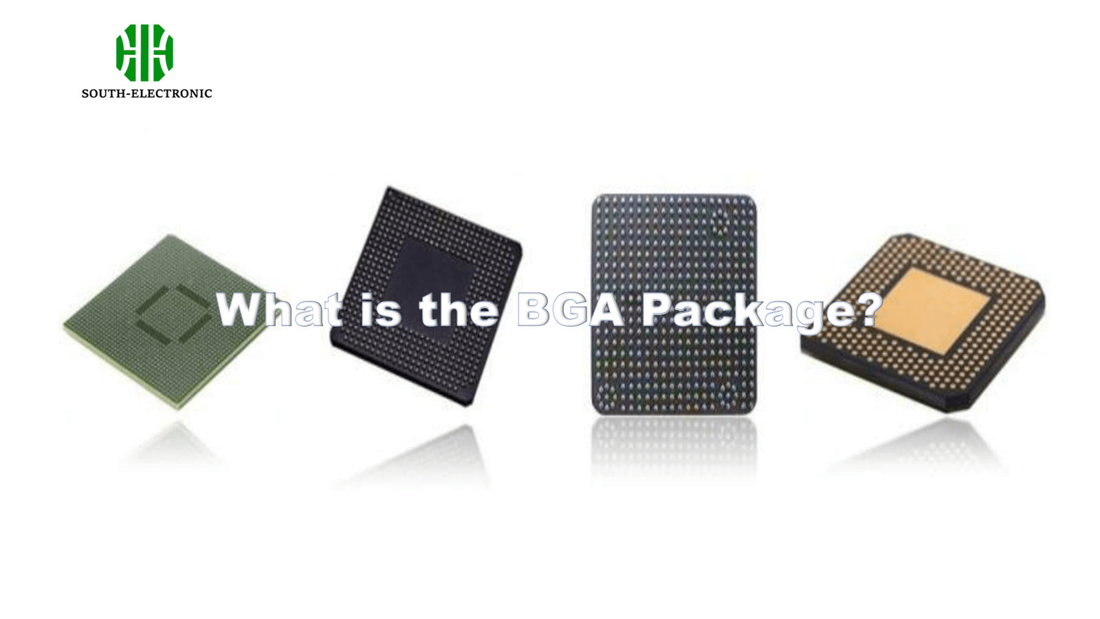
A BGA (Ball Grid Array)[^2] package arranges solder balls[^3] in grid patterns underneath integrated circuits, replacing traditional pin connections for denser PCB layouts. These tiny spheres connect chips to boards through surface-mount soldering.
While the basic concept sounds simple, BGAs revolutionized how we build modern devices. Let’s break down five crucial aspects every electronics designer should understand about these innovative packages.
What Exactly Does a BGA Package Look Like?
Ever wondered how 1,000+ connections fit on a thumbnail-sized chip? The answer hides beneath the package’s shiny surface. Traditional QFP packages use visible perimeter pins – BGAs flip that concept sideways.
A standard BGA resembles a miniature chessboard, with 0.8-1.2mm diameter solder balls placed in precise grid formations. The actual IC sits on top, while below it lies organized rows of metallic spheres ready for bonding.
| BGA Component | Typical Measurement | Advantage |
|---|---|---|
| Solder Ball Diameter | 0.2-0.8mm | Space-saving |
| Pitch (Ball Spacing) | 0.5-1.27mm | High density |
| Ball Material | Lead/Tin Alloy | Reliable melt point |
| Substrate Material | Plastic/Epoxy | Thermal stability |
Three key layers define BGA anatomy:
- Silicon Die: The actual semiconductor chip carrying circuits
- Substrate: Insulating base with conductive traces
- Solder Array: Metallic connections enabling PCB bonding
The hidden connections beneath the package allow 10x more I/Os than equivalent pin-grid designs. This secret geometry powers everything from smartphones to Mars rovers.
Why Choose BGA Over Traditional PCB Packages?
Imagine needing to connect a 500-pin processor. Through-hole packages would require a PCB the size of your palm. BGAs collapse this footprint dramatically through intelligent 3D design.
BGA[^4]s enable 70% space reduction compared to QFP packages[^5], handling complex ICs in tight spaces. Their shorter electrical paths reduce signal interference while improving heat dissipation – crucial for high-speed devices.
)
Let’s analyze critical advantages through real-world comparisons:
| Parameter | BGA | QFP (Traditional) |
|---|---|---|
| I/O Density | 400+ pins/cm² | 50-100 pins/cm² |
| Thermal Resistance | 15-35°C/W | 30-50°C/W |
| Signal Integrity | Shorter paths | Longer traces |
| Manufacturing | Automated placement | Manual alignment |
A smartphone CPU exemplifies BGA benefits:
- 14mm x 14mm package carries 1,200 connections
- Self-aligns during reflow soldering
- Handlers GHz frequencies efficiently
- Dissipates 5W+ heat reliably
While requiring specialized assembly tools, BGAs enable devices we use daily – no viable alternative exists for high-performance electronics.
Where Are BGA Packages Most Commonly Used?
Your pocket holds multiple BGA devices right now. Since their 1990s introduction, these packages became ubiquitous wherever performance meets miniaturization.
BGAs dominate 82% of advanced PCB assemblies[^6], particularly in smartphones, GPUs, automotive ECUs, and IoT devices. Their reliability under vibration makes them perfect for moving vehicles and industrial equipment.
)
Let’s explore sector-specific implementations:
| Industry | BGA Usage | Example Component |
|---|---|---|
| Consumer Electronics | Mobile SoCs, Memory Modules | Snapdragon Processors |
| Automotive | Engine Control Units (ECUs) | ABS Controllers |
| Medical | Imaging Systems | MRI Interface Cards |
| Aerospace | Avionics | Flight Control Modules |
In smartwatches:
- BGAs enable 10nm processors in 30mm²
- Withstand daily bending stresses
- Maintain connections during -20°C to 85°C swings
Even "simple" devices now use BGAs – a basic IoT sensor might contain three BGAs (MCU, radio, memory). Their prevalence grows as technology shrinks.
How to Design PCBs for BGA Components?
Attempting your first BGA layout? Unlike through-hole parts, these packages demand precision planning. One misplaced via could ruin the entire assembly.
Design BGAs with adequate escape routing space, using micro-vias for high-density connections. Apply thermal relief patterns and follow IPC-7351 standards for pad sizing and spacing.
)
Implement these critical steps:
-
Pad Design
- Match ball pitch (common mistake: 0.5mm pads for 0.8mm balls)
- Use NSMD (Non-Solder Mask Defined) pads for alignment
-
Routing Strategy
- Escape routes between peripheral balls first
- Staggered via-in-pad for dense grids
- 45° trace angles reduce impedance
-
Thermal Management
- Thermal vias under hot components
- Copper balance to prevent warping
A proper design checklist includes:
- 20% pad size larger than balls
- 3:1 via aspect ratio maximum
- 0.1mm solder mask clearance
- No traces in keep-out zones
Advanced designs use HDI (High Density Interconnect) tech with laser-drilled microvias. Always prototype before full production.
Can You Repair BGA Devices?
Dropped your phone and now it won’t boot? BGA repair[^7] is possible but requires specialized equipment. Those tiny balls can’t be hand-soldered like through-hole components.
Professional BGA rework station[^8]s use precise heat controls and optical alignment to replace damaged packages. Success rates exceed 85% with proper tools, though DIY attempts often cause further damage.
)
Repair Process Breakdown:
| Step | Tools Needed | Critical Parameters |
|---|---|---|
| Removal | Hot air gun + Thermocouple | 215-235°C peak temp |
| Site Cleanup | Copper braid + Flux | 0°C-5°C/sec cool rate |
| Ball Replacement | Stencil + Solder paste | 0.1mm ball placement |
| Reflow | IR Preheater + Nozzle | Ramp rate 1-3°C/sec |
Common mistakes to avoid:
- Overheating neighboring components
- Using wrong solder ball alloy
- Misaligning during placement
- Insufficient preheating causing warping
While possible, BGA repair remains challenging. For mission-critical devices, consult certified specialists instead of attempting fixes yourself.
Conclusion
BGA packaging revolutionized electronics through dense, reliable connections. From design rules to repair techniques, mastering BGAs unlocks possibilities in modern PCB development. Their dominance ensures relevance in evolving tech landscapes.
[^1]: Discover the advantages of high-density packaging and how it optimizes space in electronic devices.
[^2]: Explore this link to understand the revolutionary design of BGA packages and their impact on modern electronics.
[^3]: Learn about the crucial role of solder balls in BGA packages and their significance in circuit design.
[^4]: Explore the benefits of BGA packages to understand why they are preferred in modern electronics for performance and space efficiency.
[^5]: Learn about QFP packages and their limitations compared to BGAs, crucial for making informed design choices in electronics.
[^6]: Discover the prevalence of BGA technology in PCB assemblies and its impact on modern electronic devices.
[^7]: This resource will provide insights into effective BGA repair techniques and best practices for successful outcomes.
[^8]: Explore this link to understand the technology behind BGA rework stations and their importance in electronic repairs.


