

Ever struggled to pick PCB via types? Wrong choices bring signal issues or waste space. I’ve seen costly redesigns from rushed via decisions. Let me untangle this mess for you.
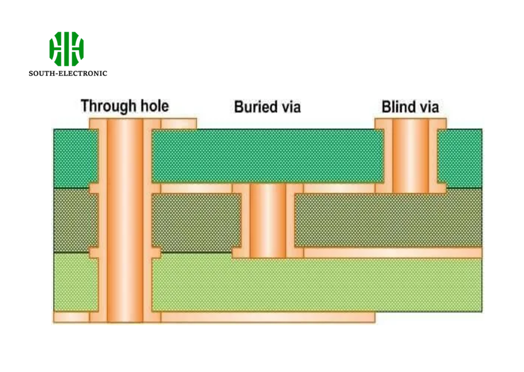
Choose based on cost, board density, and speed needs. Through vias work for simple, low-cost boards. Blind vias free surface space in complex designs. Buried vias isolate high-speed signals but raise costs. Always balance tradeoffs.
Now you know the framework. But several key sub-questions will help master this skill. We’ll tackle them step-by-step.
What factors determine the perfect via size in circuit board design?
Guessing via sizes invites failures. I burnt a prototype last year from undersized vias. Stop gambling – use critical factors instead.
First match size to current load and heat flow. Then check manufacturing limits. Finally, see how spacing affects routing density. Never exceed fabrication minimums or overload capacity.
Three Primary Size-Drivers
Balancing these prevents failure:
| Factor | Small Via Impact | Large Via Impact | Sweet Spot |
|---|---|---|---|
| Current/Signal | Overheats or chokes speed | Wasted space | Match trace width + 20% margin |
| Manufacturing | Risk of incomplete plating | Higher drilling cost | Respect fab shop drill charts |
| Space/Density | Allows tighter components | Blocks routing channels | Use smallest reliable size in dense zones |
High-current paths like power rails need larger diameters – I aim for 0.3mm minimum. For signals below 100MHz, 0.2mm often suffices. Thermal vias transfer heat; cluster small ones under hotspots. Always account for plating thickness. A 0.1mm hole finishes at 0.08mm after copper deposition. Check your fabricator’s capabilities first. They can etch fine lines differently than competitors. Density-driven designs benefit from micro-vias at 0.1mm in advanced HDI processes. But standard boards rarely need this.
What is the difference between via and contact?
Mixing pads and vias causes assembly nightmares. I once debugged for weeks due to mislabelled contacts. Learn precise differences to avoid pain.
Vias connect PCB layers internally without soldering. Contacts (pads) attach component leads to the surface. Pads actively join circuits; vias passively route them.
Functional Break-Down
Core use cases explained:
| Feature | Via Function | Contact (Pad) Function | Critical Distinction |
|---|---|---|---|
| Location | Any layer junction | Outer surfaces only | Pads require solder access |
| Solder Use | None if plugged | Must accept solder | Solder adhesion defines pads |
| Thermal Role | Passive heat transfer | Active component cooling | Pads directly touch components |
| Reliability | Vulnerable to barrel cracks | Risk is pin detachment | Stress points differ in testing |
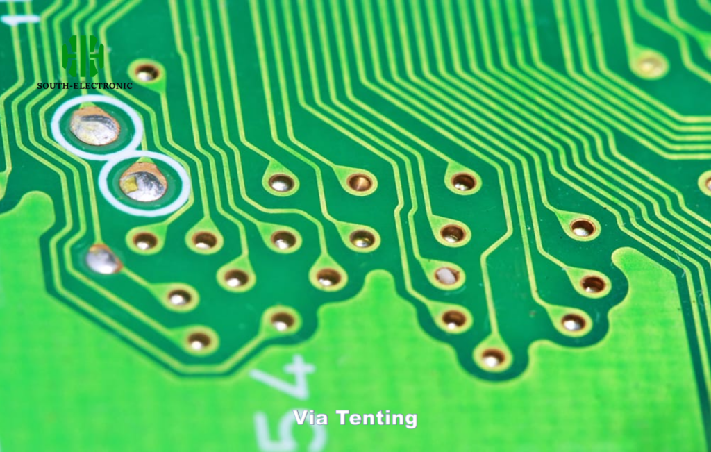
Vias transfer signals between layers without surface attachment. Pads anchor components to complete circuits. A plated hole stays a via until you solder to it – then it becomes a contact. Blind/buried vias avoid surface pads entirely. I reserve contacts only for components like IC pins or connectors. For high-pin-count chips, tented vias save space but can’t be soldered. Test points illustrate hybrid designs: via holes doubling as probe contacts.
Why Do Circuit Board Vias Fail?
Failing vias kill boards silently months later. In our workshop, cracked barrels caused 29% of field returns. Protect your work with cause analysis.
Main causes are thermal cycling stress and manufacturing defects. Plating voids or drill misalignment start hidden weaknesses. Mechanical torsion then cracks them.
Root Cause Breakdown
Prevent through design rules:
| Failure Trigger | How It Happens | Critical Prevention Step |
|---|---|---|
| Thermal Stress | Repeated expansion cracks barrel | Match hole size to board thickness |
| Plating Voids | Weak copper cracks under load | Specify 25µm+ plating thickness |
| Drill Damage | Overheating delaminates holes | Control drill RPM and feed rates |
| Moisture | Trapped steam pops plating | Bake boards before assembly |
Vias fail where stresses concentrate. Thin plating splits during temperature swings – measure copper coverage in cross-sections. I avoid micro-vias in flexible zones; barrel depth matters under bending forces. For lead-free soldering, watch peak temperatures above 260°C. Always derate via size versus technical specs to cover tolerance drifts. Use plugged vias in BGA areas so solder doesn’t wick away. X-ray inspection catches voids before shipping. Design vias away from bend lines and mounting screws.
Conclusion
Match via types to cost, density, and layer needs. Test critical vias for thermal stress. Always prioritize your manufacturer’s capabilities first.

