
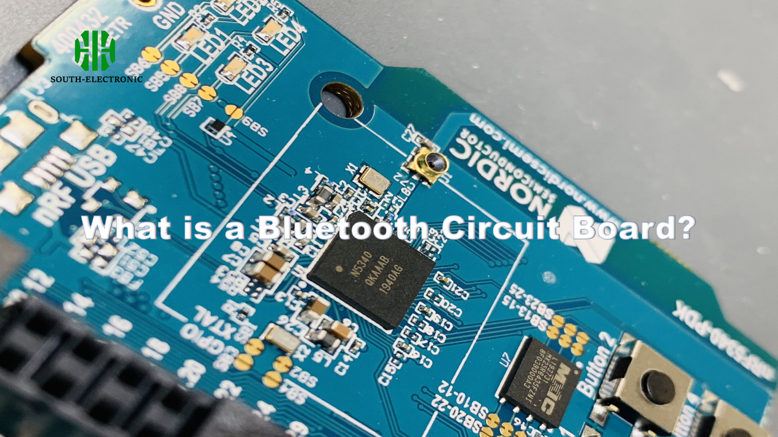
Tired of tangled cables limiting your device connectivity? Bluetooth circuit board[^1]s solve this by enabling wireless communication through compact, integrated designs. Let’s explore what makes these boards tick and why they power modern wireless tech.
A Bluetooth circuit board integrates antenna, radio chips, and microcontrollers to enable short-range wireless communication between devices (typically up to 100 meters) using 2.4 GHz radio waves[^2]. These printed circuit boards (PCBs) form the backbone of wireless speakers, wearables, and smart home devices.
While basic Bluetooth functionality seems simple, engineering these boards requires balancing signal strength, power efficiency, and physical space constraints. Let’s break down key design and operational aspects through critical questions.
How Does a Bluetooth Circuit Board Transmit Wireless Signals?
Lose connection when your wireless earbuds are just 10 feet away? Signal transmission quality depends on three core PCB elements working in harmony.
Bluetooth boards convert data into 2.4 GHz radio waves via built-in antennas, using frequency-hopping spread spectrum (FHSS) technology[^3] to avoid interference with other wireless devices. The system alternates between 79 channels 1,600 times per second.
)
Three Key Transmission Components
| Component | Role | Design Impact |
|---|---|---|
| RF Transceiver | Converts digital signals to radio waves | Requires impedance-matched traces |
| Antenna | Radiates electromagnetic waves | Shape/length determines frequency range |
| Balun Circuit | Matches antenna to transmitter | Prevents signal reflection losses |
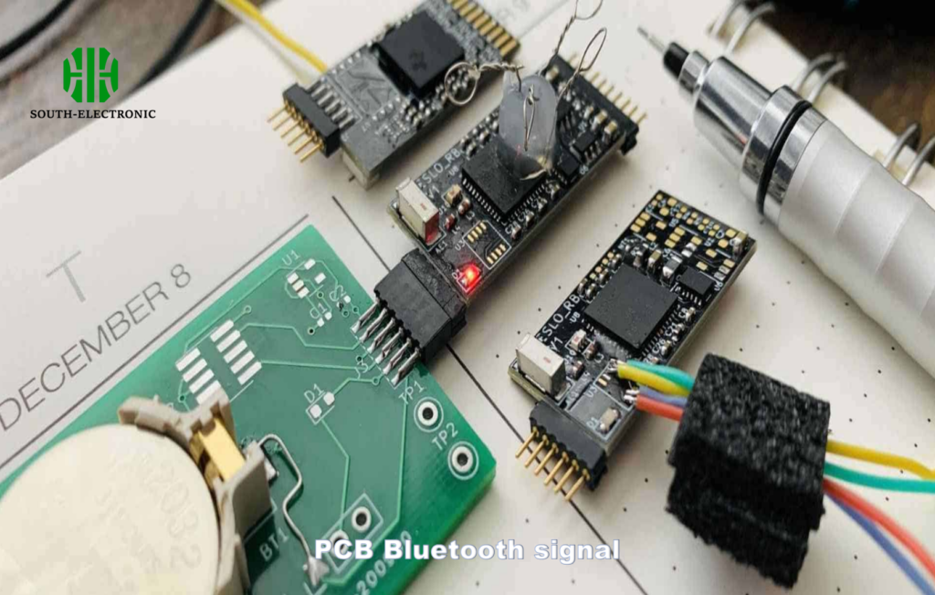
Bluetooth signal strength depends heavily on the antenna design. I once built a fitness tracker prototype where a 5mm antenna length error reduced range by 40%. Engineers optimize antenna shapes (chip, PCB trace, or external wire) based on device size and power limits. Proper ground plane placement prevents signal absorption by nearby metal components.
What Components Are Critical for Bluetooth PCB Reliability?
Experiencing random disconnects even at close range? Poor component selection or layout creates most Bluetooth reliability issues.
Critical Bluetooth PCB components include: Bluetooth IC/module, crystal oscillator, RF front-end, and impedance-controlled microstrip traces. Each contributes to stable wireless performance and must meet tight specifications.
)
Reliability Factors Chart
| Factor | Ideal Spec | Failure Impact |
|---|---|---|
| Impedance Matching | 50Ω ±10% | Signal reflection >30% loss |
| Crystal Tolerance | ±10ppm | Frequency drift breaks pairing |
| Power Supply Noise | <30mV ripple | Random disconnects |
| Thermal Stability | -40°C to +85°C | Range reduction in hot/cold |
During my first Bluetooth speaker project, a 3-cent power regulator replacement solved 90% of dropout issues. High-quality decoupling capacitors near the Bluetooth IC are non-negotiable – I use at least one 1µF and one 10nF cap in parallel. Temperature testing revealed that cheap crystal oscillator[^4]s drift beyond usable range in car dashboards during summer.
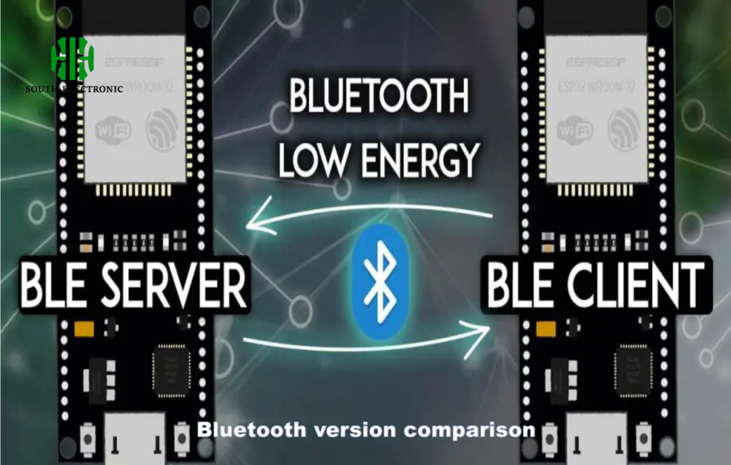
When Should You Choose Bluetooth 5.0 vs Classic Bluetooth PCBs?
Confused about Bluetooth versions for your project? The choice depends on data needs rather than just chasing the newest standard.
Use Bluetooth 5.0[^5] PCBs for IoT devices needing long range (up to 240m) or high throughput (2Mbps), and Classic Bluetooth (BR/EDR) for audio streaming where legacy compatibility matters. Version 5.0 consumes 50-80% less power for intermittent data.
)
Version Selection Matrix
| Parameter | Classic (BR/EDR) | Bluetooth 5.0 |
|---|---|---|
| Max Data Rate | 3 Mbps | 2 Mbps (LE) |
| Max Range | 100m | 240m (LE) |
| Power Use | Higher | Lower (LE mode) |
| Latency | <60ms | Varies (3-6ms achievable) |
| Device Support | Universal | Requires 4.0+ devices |
A client insisted on BT5 for a basic remote control – wasted $12/unit on unnecessary capabilities. Conversely, a warehouse inventory tracker using BT5's long-range mode achieved 180m connectivity through metal racks. Remember: audio projects usually need classic Bluetooth for HSP/HFP/APTX support.
Why Do Manufacturing Tolerances Affect Bluetooth Signal Range?
Your prototypes work perfectly, but production units fail certification? Bluetooth PCBs demand tighter tolerances[^6] than typical boards.
A 0.1mm trace width error on Bluetooth PCBs can cause 10-25% signal loss due to impedance mismatch. Tight controls on dielectric thickness (±5%) and copper roughness maintain high-frequency performance.
%[PCB manufacturing inspection](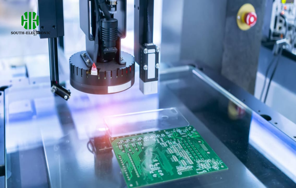 )
)
Tolerance Impact Analysis
| Parameter | Allowed Tolerance | Impact per 1% Error |
|---|---|---|
| Trace Width | ±5% | 0.5Ω impedance change |
| Dielectric Thickness | ±3% | 1.2% velocity shift |
| Copper Roughness | <3µm RMS | 0.8dB loss at 2.4GHz |
| Solder Mask Thickness | ±10µm | Capacitance variance |
After a batch failure from 8% dielectric variation, we now specify Isola FR408HR laminate instead of standard FR4 for better consistency. Impedance testing with $25k TDR equipment pays for itself by avoiding 15% scrap rates in high-frequency boards. Even solder mask color affects performance – green performs better than black due to lower loss tangent.
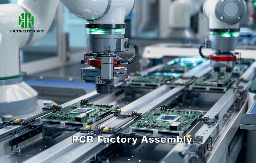
How Much Does Custom Bluetooth PCB Assembly Cost?
Sticker shock from your first Bluetooth PCB quote? Costs range from $3/unit for basic boards to $200+ for medical-grade designs. Let’s break down the factors.
Basic 2-layer Bluetooth PCBs cost $2-8/unit in 1k quantities, while RF-optimized 4-layer boards with FCC certification hit $15-50/unit. Complex designs needing shielded housings or antenna tuning cost more.
)
Cost Breakdown Table
| Cost Factor | Low End | High End |
|---|---|---|
| Layers | $1/layer | $4/layer (RF materials) |
| Components | $0.50 (basic IC) | $22 (certified BT5.2 module) |
| Testing | None | $8/unit (RF parametric) |
| Certification | $0 (self-declare) | $15k (FCC/CE full) |
| Minimum Order | 50pcs ($150) | 1k pcs ($25k+) |
My team recently paid $7.30/unit for 500 medical chest straps: 4-layer Taconic PCB ($3.20), Nordic nRF52840 ($4.10), and basic FCC testing ($0.80). Avoid "RF expert" upcharges by providing complete Gerber and IPC-6012E Class 2 specs upfront. For prototypes, JLCPCB’s $2 Bluetooth boards work if you handle antenna tuning yourself.
Conclusion
Bluetooth PCBs merge RF engineering with cost-effective manufacturing. Success requires balancing signal integrity, component selection, and production tolerances while matching Bluetooth versions to actual use cases. Choose experienced assemblers and always budget for proper RF testing.
[^1]: Understanding Bluetooth circuit boards is essential for grasping modern wireless technology. Explore this link to deepen your knowledge.
[^2]: 2.4 GHz radio waves are crucial for wireless communication. Discover their applications and significance in technology by exploring this resource.
[^3]: FHSS technology is vital for reducing interference in wireless communication. Learn more about its workings and benefits through this link.
[^4]: Exploring the impact of crystal oscillators can help you avoid frequency drift issues and improve Bluetooth reliability.
[^5]: Learning about Bluetooth 5.0’s benefits can guide your project decisions, especially for IoT applications requiring long range and high throughput.
[^6]: Learn how maintaining tighter tolerances can significantly enhance Bluetooth signal performance and reduce production failures.

