
What is a multilayer PCB?
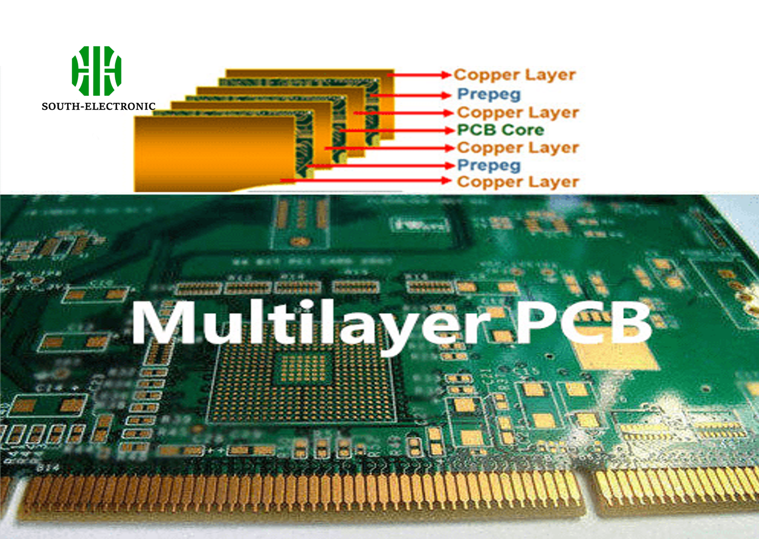
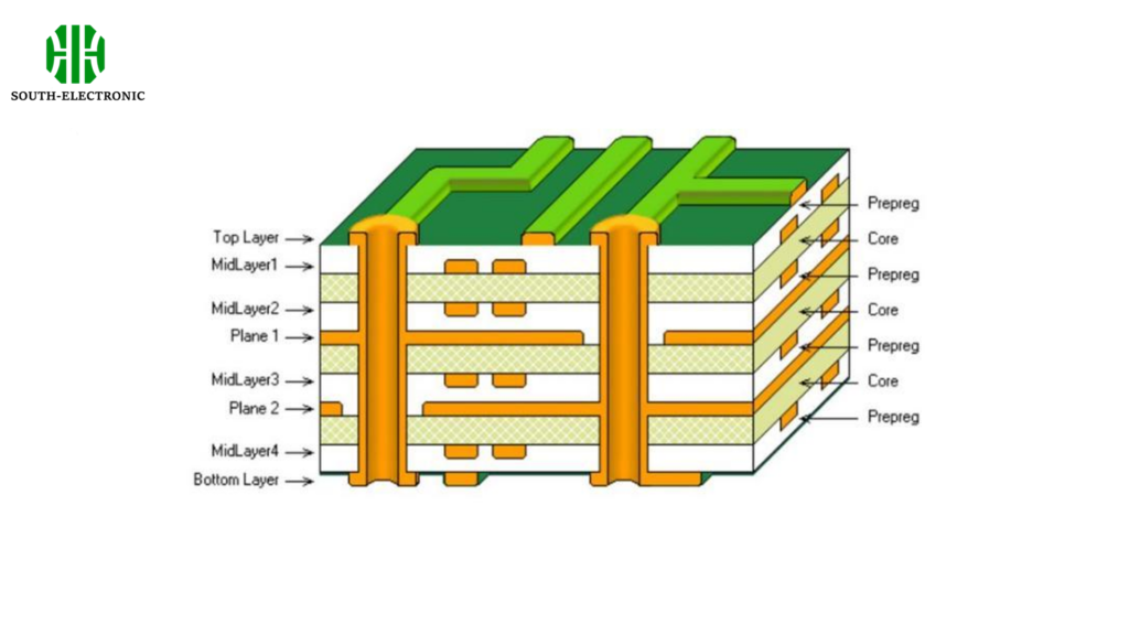
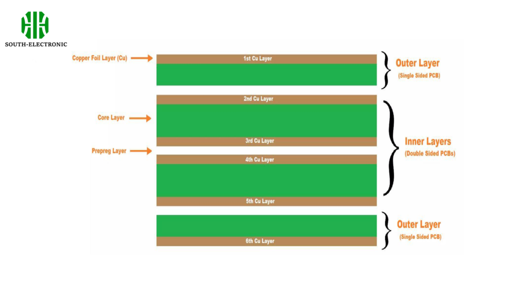
A multilayer PCB (Printed Circuit Board) is a highly complex type of circuit board. It consists of three or more conductive layers of copper, each separated by and bonded together with layers of insulating material. These layers are then pressed together under high temperatures and pressures to create a single, integrated structure. The internal layers are interconnected through vias, which are tiny holes that are drilled and plated with copper to form electrical connections between the different layers. This configuration allows for denser and more complex circuitry within a smaller footprint than single-layer or double-sided PCBs.
Layer Functions in Multilayer PCB
| Layer Number | Function | Common Materials |
|---|---|---|
| 1 | External Signal Layer | Copper, Standard or High-TG FR-4 |
| 2 | Internal Signal Layers | Copper, High-TG FR-4, Prepreg |
| 3 | Ground Plane | Copper, FR-4 |
| 4 | Power Plane | Copper, Prepreg |
| 5+ | Additional Signal/Power Layers | Copper, High-TG FR-4, PTFE (Teflon), Rogers Materials |
Multilayer PCBs are used in a variety of high-demand sectors because of their advanced capabilities:
- Consumer Electronics: Smartphones, computers, and other personal devices.
- Medical Devices: Advanced diagnostic and imaging equipment.
- Automotive Industry: Systems requiring high reliability under harsh conditions, such as engine controls and infotainment systems.
- Military and Aerospace: Applications where maximum performance and reliability are critical in extreme conditions.
Single-Layer vs.Double-sided PCB vs.Multilayer PCB: What’s the Difference?
Single-Layer PCB
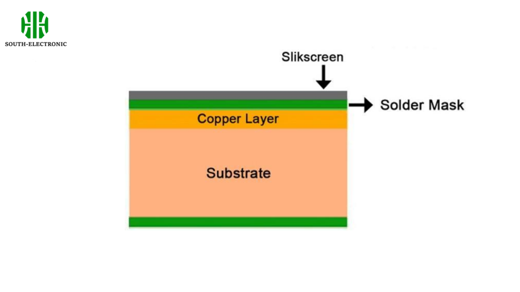
- Definition: Single-layer or single-sided PCBs have one conductive layer of material, typically copper, which is mounted on one side of the board. The other side holds the electronic components.
- Applications: Single-layer PCBs are suitable only for simple devices due to space constraints for routing. They are common in simpler consumer electronics like calculators, printers, and power supplies.
Double-Sided PCB
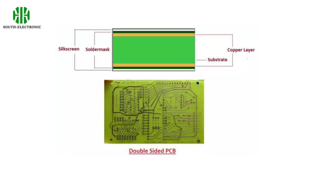
- Definition: Double-sided PCBs have conductive copper layers on both sides of the board, allowing circuits to cross over each other, increasing the density without a significant cost increase.
- Applications: They require additional steps such as through-hole plating to connect the layers. They are used in more complex systems than single-layer PCBs can handle, like HVAC systems and automotive dashboards.
Multilayer PCB
- Definition: Multilayer PCBs consist of three or more double-sided boards separated by insulation, usually pressed together. They can have anywhere from 4 to 12 layers or more, with some specialized versions having up to 40 layers.
- Applications: The priciest kind of PCB because of the complicated manufacturing processes involved. It’s usually used in high-end electronics where space, weight, and performance are crucial, such as smartphones, computers, and military and medical equipment.
Advantages of Multilayer PCB
Multilayer PCBs offer several significant advantages over their simpler counterparts:
- Enhanced Durability and Reliability: Additional layers provide greater protection against environmental stresses.
- High Density and Compact Size: Enables more features in smaller devices, crucial for modern electronics.
- Improved Signal Integrity: Reduced electromagnetic interference due to internal shielding layers.
Design Considerations for Multilayer PCB
- Layer Stackup and Configuration: Ensure symmetrical layering to minimize EMI and maintain structural integrity. This helps in thermal management and signal integrity.
- Material Selection: Choose substrate materials like FR-4 or advanced composites for specific electrical and thermal performance requirements.
- Signal and Power Integrity: Implement controlled impedance, proper routing, and adequate decoupling to maintain signal clarity and stable power distribution.
- Thermal Management: Use thermal vias and materials that help dissipate heat to keep your components from overheating.
- Manufacturability and Testing: Design with manufacturing in mind and make sure you have accessible test points for easier debugging and quality control.
Multilayer PCBs are a critical component in many of the devices we use every day, from smartphones to military equipment. They allow for more functionality in a smaller space, increase the reliability of the device, and keep everything running smoothly.

