
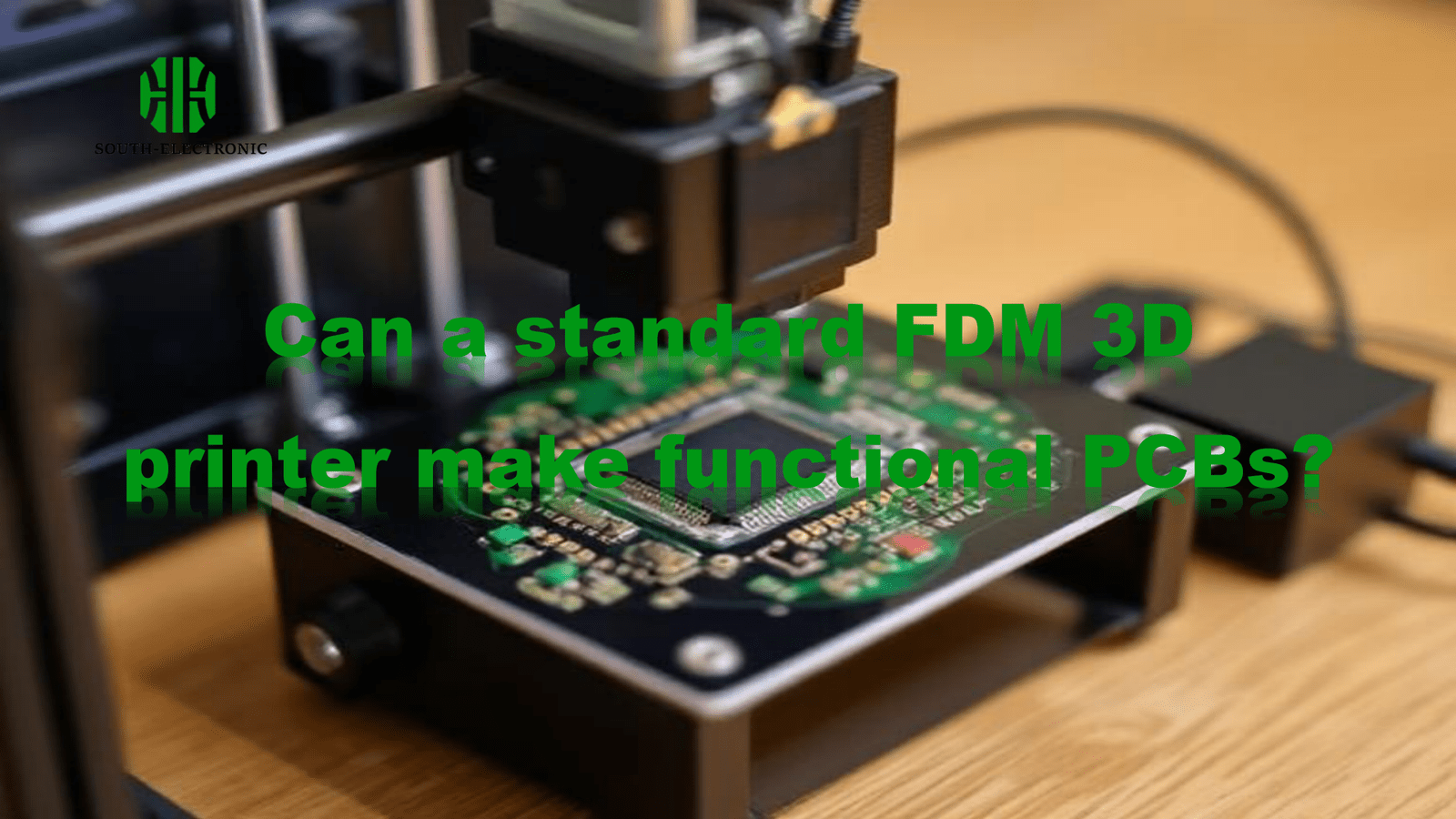
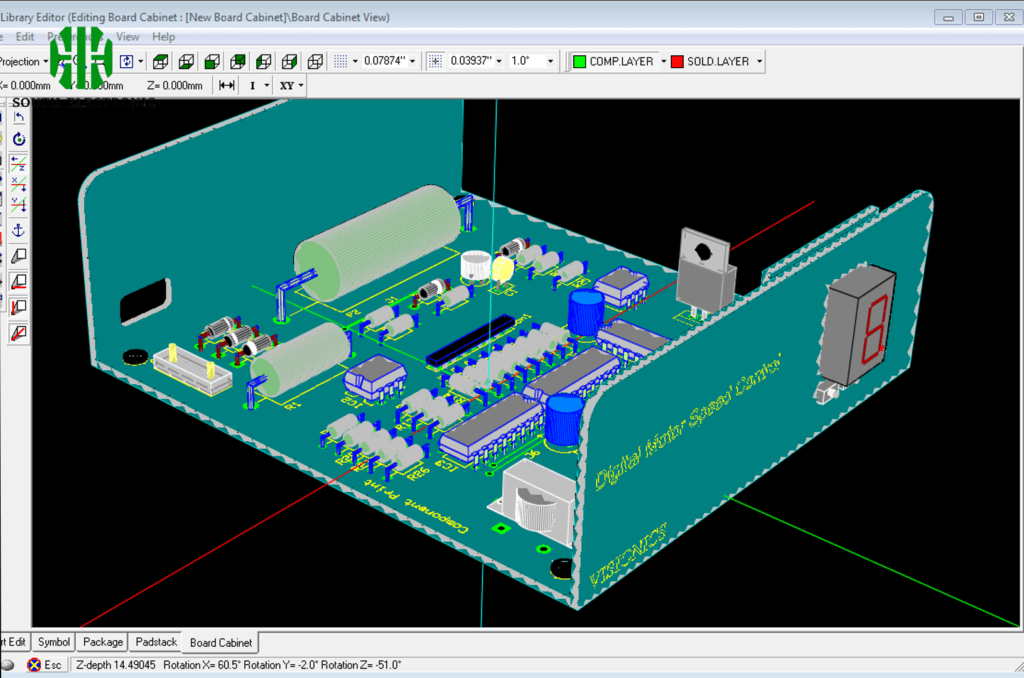
You need circuit boards now, but traditional PCB processes take weeks. Frustrating delays stall your projects. Let me show you how your FDM printer solves this.
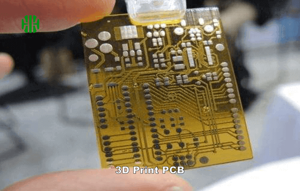
Yes, standard FDM printers can create working PCBs using conductive filaments[^1], but with limitations. Traces may conduct poorly, and soldering components poses challenges. This method suits low-current prototypes needing quick iterations.
While exciting, practical hurdles exist. Understanding these lets you decide when printed PCBs work best or when alternatives shine. Let’s uncover realities beneath the surface.
Why won’t PCB traces conduct or components solder?
Struggling with non-conductive traces? Filament limitations create this headache. Your excitement turns to frustration when circuits remain dead.
Conductive filament resistance is 100X higher than copper. Soldering melts plastic bases at 200°C. Mitigate with wide traces, low-temp solder, or press-fit connectors.
Material Limitations Explained
Conductive filaments contain metal/carbon particles in plastic. This hybrid structure causes fundamental performance trade-offs:
-
Electrical Issues:
- Resistance rises dramatically over trace lengths
- Current handling maxes around 200mA
- Signal degradation above 10kHz frequencies
-
Thermal Challenges:
- ABS/PLA bases melt below soldering temperatures
- Heat sinks needed near components
- Annealing reduces warping but adds steps
| Failure Cause | Underlying Reason | Practical Solution |
|---|---|---|
| High Resistance | Low conductive filler ratio | 4mm+ trace widths |
| Solder Adhesion Fail | Polymer melting point | Sub-200°C alloys + flux |
| Component Detachment | Thermal expansion mismatch | Epoxy reinforcement |
Filament storage matters too. Moisture absorption degrades conductivity over time. Use sealed containers with desiccant for best results between prints. These constraints make 3d printed PCBs best for basic switching applications under 12V.
Can 3D-printed PCBs[^2] save time and money for prototyping?
Waiting days for factory boards kills momentum. Costs pile up with every design change. Instant in-house printing changes the game.
Printed PCBs save 90% cost and 80% time for early prototypes. No minimum orders or shipping delays. Complex shapes impossible with standard PCB come free.
Detailed Cost-Benefit Breakdown
Let’s quantify savings from your 3d printer pcb printing setup:
Cost Factors (Per Board):
- Material: $0.50 conductive filament + $0.20 substrate
- Energy: <$0.10 electricity (4-hour print)
- Labor: 15 minutes active work vs 3 days lead time
Traditional PCB Comparison:
- $50 setup fees + $8 shipping (basic 2-layer)
- 5-15 day production timelines
- $15+/board order quantities under 10
Time Trade-offs Table:
| Stage | 3d printed pcb | Traditional pcb |
|---|---|---|
| Design to Print | 1-6 hours | 24+ hours |
| Re-spin cycles | Immediate | 3+ days each |
| Shape Complexity | Unlimited | Rectangular only |
Your 3d printer pcb printing excels when testing core functionality matters most. You trade electrical perfection for radical iteration speed. Just avoid high-frequency or power-hungry circuits.
What other ways are there to 3D print PCBs?
FDM frustrations making you quit? Better methods exist. Beyond conductive filament lie professional solutions with copper-like results.
Alternative approaches include electroplating FDM traces[^3], hybrid CNC printing, and direct-ink-write systems. These boost conductivity 10X but require extra tools/materials.
Emerging Method Comparison
Each technique solves different aspects of pcb 3d printer challenges:
Electroplating Enhancement
- Print insulating base with deep channels
- Fill grooves with conductive paste
- Electroplate copper onto paste
- Pros: Near-standard conductivity
- Cons: Added chemicals and equipment
Integrated Hybrid Systems
- Print substrate then mill copper clad
- Laser-selectively deposit conductive ink
- Combined FDM/inkjet commercial machines
| Method | Conductivity | Equipment Cost | Best Use Case |
|---|---|---|---|
| Basic FDM Printing | Low | $200-$500 | Learning, LEDs |
| Electroplated Traces | Medium | $500+ | Arduino-level signals |
| Professional Direct-Write | High | $2000+ | RF circuits |
While multi-material printers like Voxel8 exist, most makers combine tools creatively. Example: Print base shape with FDM, then hand-fill traces with silver epoxy for moderate conductivity boosts without huge investments.
Conclusion
FDM printers create functional but limited 3d printed circuit boards. Perfect for quick, low-power prototypes. For complex needs, explore enhanced printing or hybrid methods.
[^1]: Explore how conductive filaments can enhance your 3D printing projects and their applications in creating functional prototypes.
[^2]: Learn about the advantages and limitations of 3D-printed PCBs versus traditional methods for better decision-making in prototyping.
[^3]: Discover the process of electroplating FDM traces and how it can significantly enhance the performance of your 3D-printed circuits.


