
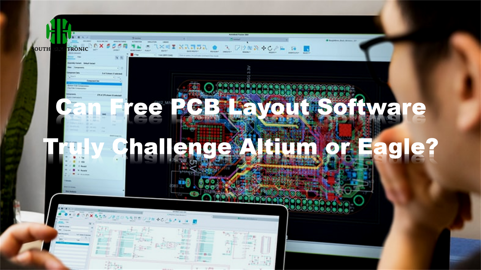
You need to design a circuit board but have no budget. Paid tools feel out of reach. Free pcb layout software promises hope. But does it deliver against giants like Altium or Eagle?
While free pcb drawing software helps beginners start pcb design without cost, it rarely matches commercial tools in complex tasks. Key limitations include restricted layers and board sizes in free versions, making them unsuitable for professional-grade printed circuit board design software projects.
Now, we’ll uncover the reality behind free tools. You’ll see where they shine and where they crash. Let’s tackle your biggest questions about modern pcb design online.
Is Open Source PCB Design Worth The Learning Curve?
You’ve spent weekends fighting confusing tool interfaces. Open source pcb design software seems complex. Is it truly worth your precious hours?
Learning free printed circuit board design software brings value despite obstacles. You gain fundamental skills and adapt without costs, though mastery takes practice. The investment pays off for small projects and prototypes.

Critical Choices for Self-Taught Designers
Let’s break this into core questions. First, why struggle with open source tools? You build skills that transfer to any software. Free versions like KiCad won’t lock your files behind subscriptions. They teach routing rules and layer management from scratch. Second, when do the struggles outweigh benefits? Your project complexity decides this. Consider these key trade-offs:
| Learning Factor | Advantage | Challenge |
|---|---|---|
| Skill Building | Universal troubleshooting knowledge | Weeks needed for basic competence |
| Feature Freedom | No artificial export limits | Critical tool automation missing |
| Resource Scarcity | Community forums for free help | Fewer step-by-step tutorials |
Time required varies highly. Simple boards might need ten hours of study. Multi-layer projects could take fifty. If you aim for professional work, you’ll eventually hit barriers. The free tools often lack advanced signal analysis. This forces manual error checks. Remember that basic pcb design skills remain valuable, even if you upgrade later. Your effort stays anchored in learning fundamentals.
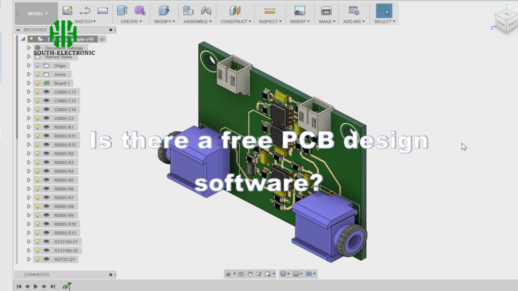
Free PCB Design Tools: What Are the Hidden Limitations to Watch For?
Free tools tempt you with zero costs. Suddenly, your project stalls at export. Why? Unadvertised limits sabotage complex pcb design work.
Watch for boundaries in layers and dimensions first. Many free pcb drawing software versions cap board size or copper layers. These silently restrict what you can build or output professionally.
Decoding Invisible Boundaries
Free plans aren’t evil. They suit small projects beautifully. But you can’t ignore four key barriers:
- Board Dimensions: Most free tools limit you to 10x8cm boards. Need a guitar pedal PCB? Fine. Dreaming of a drone controller? Impossible.
- Layer Count: Free tiers usually allow two copper layers. High-speed designs need four or six. You’ll face noise issues without that freedom.
- Library Access: Commercial tools offer certified footprints. Free pcb layout software often makes you build parts manually. One wrong solder pad ruins your board.
- Gerber Generation: Some enforce watermarks on fabrication files. Manufacturers might reject these. Your prototypes become useless.
Always test file exports early. I learned this when a free tool blocked panelization for mass production. Now I validate limits during schematic capture. Free pcb design online saves cash but costs time in workarounds.
How to Collaborate and Go From Schematic to Gerber Online?
You email PCB files to teammates. Chaos ensues with misplaced feedback. Modern pcb design online promises seamless teamwork. But does it actually work?
Cloud-based free pcb layout software enables live editing and commenting. You can share links instead of files. This fixes version conflicts when going from schematic to Gerber outputs.
Teamwork Without Tears
Three pillars define collaboration success. First, tool choice matters. Browser-based options like EasyEDA let everyone join instantly. No installs mean fewer excuses. Second, workflow stages need controls. Review each milestone:
- Schematic Stage: Debate component choices openly
- Routing Phase: Lock layers during critical traces
- Final Export: Validate Gerbers together before sending to fabricators
Third, trust but verify. I once lost days due to untracked changes in a DIY project. Now I enforce change logs in shared projects. Free tools shine here. They offer automatic version histories. But caution remains. Without cloud backups, one accidental delete sets you back hours. Balance freedom with process discipline. This method transforms confusing messes into coordinated projects using free pcb design resources.
Top Mistakes Beginners Make and How Software Choices Can Help Avoid Them?
Your first PCB arrives nonfunctional. Solder pads short circuit. Was the manufacturer faulty? Probably not. Basic errors plague newcomers in pcb design.
You create electrical issues through ignorance. Wrong trace widths or clearance gaps damage circuits. Free tools with auto-check rules prevent such failures before fabrication.

Foolproofing Your Learning Curve
Start by understanding mistake patterns. Then use software features as shields. Focus on these trouble zones:
- DFM Disasters: Ignoring manufacturer capabilities causes unbuildable boards
- Signal Noise: Poor grounding schemes disrupt fragile circuits
- Library Errors: Incorrect footprints make components unfittable
Free pcb drawing software like DesignSpark has design rule checks (DRC). Enable them religiously. They flag spacing violations like 0.2mm gaps that factories reject. Paid tools catch subtler timing issues, but free versions block 80% of beginner errors. I created a comparison table of protections by tier:
| Error Type | Free Software Guard | Paid Software Advantage |
|---|---|---|
| Trace Shorts | Basic clearance rules | Advanced short-circuit prediction |
| Footprint Mismatches | Manual library checks | Automated part validation tools |
| Thermal Stress | Limited warnings | Simulation-driven hotspot alerts |
| Power Spikes | No prevention | Voltage drop analysis tools |
Always simulate high-current paths manually if using free tools. Print paper templates to verify footprints. These habits compensate for feature gaps.
Conclusion
Free PCB tools help beginners start affordably but struggle with complex jobs. Smart choices avoid frustration. Use them tactically for small designs while learning.

