
How to Start Your First PCB Design?
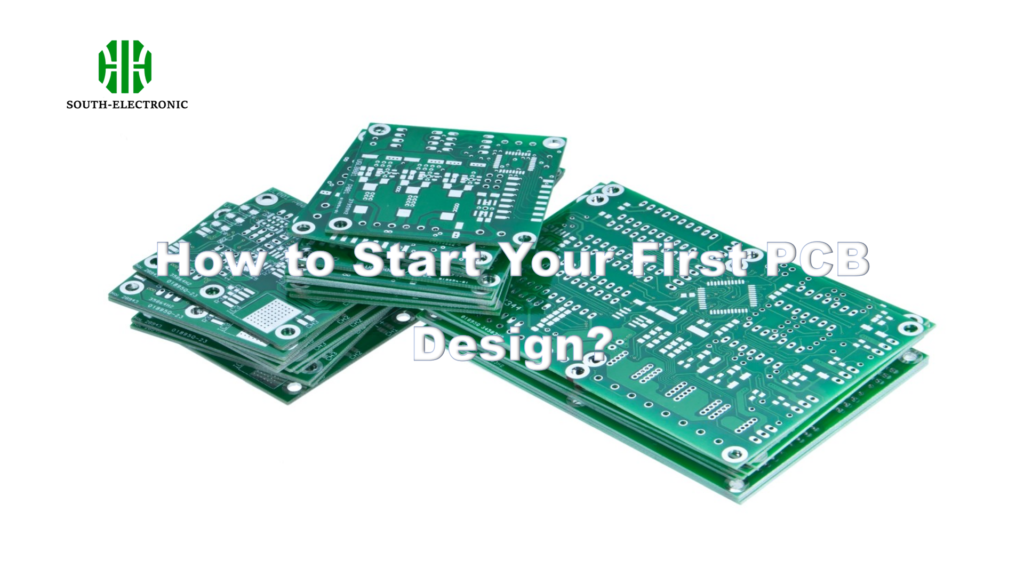
Free step-by-step PCB design guide for beginners: Learn software selection, avoid fatal layout errors, and prepare manufacturing files correctly to save time & money.
What Are the 7 Critical Stages in a Professional PCB Assembly Process?
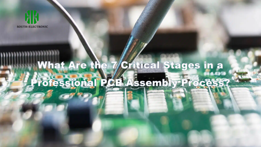
Master 7 PCB assembly stages to avoid delays. Choose IATF/ISO-certified manufacturers for medical/auto projects, fix critical design errors early & know when to switch from DIY to pro assembly.
What Are the Most Common Causes of PCB Failure?
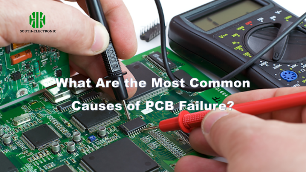
Diagnose & prevent common PCB failures: manufacturing flaws, environmental stress, soldering defects. Learn visual inspection, repair techniques & cost-effective solutions.
Stuck with SMT Assembly Defects?
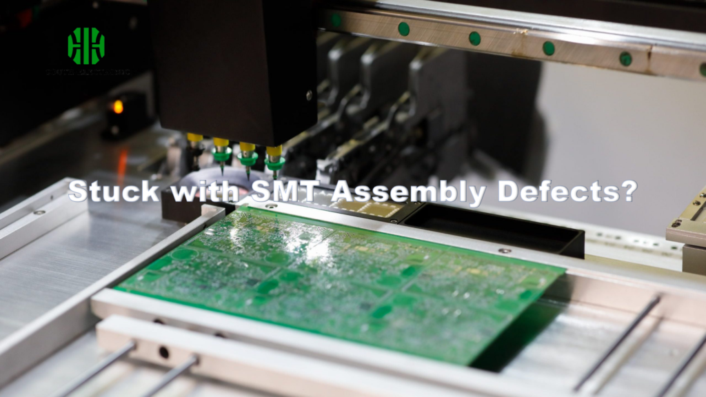
Avoid SMT prototype fails! Top defects (tombstoning, bridging, BGA issues) with fixes. Key: design audits, communication with assembly shops & pre-testing. Save costs & time.
What Exactly is a PCB Trace?
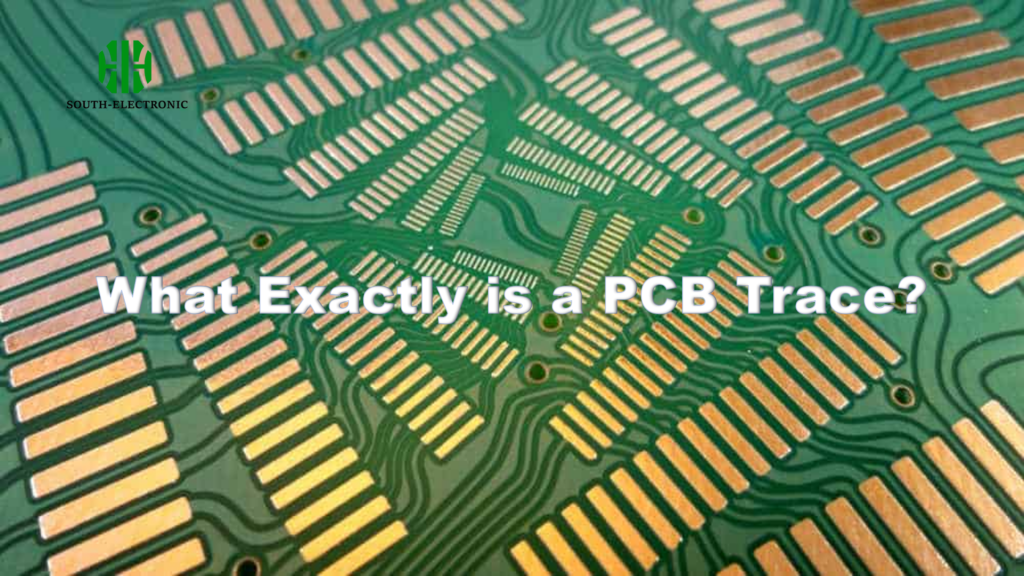
Discover why PCB traces fail—impedance issues, overheating—and how to fix them. Learn trace design factors, troubleshooting steps, and tools for reliable circuits.
How to Test a Diode?
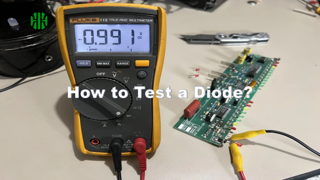
Learn to test diodes with any multimeter: Set to diode/resistance mode, probe anode/cathode. Identify healthy (0.5-0.8V drop) vs faulty diodes (shorted/open/leaky). Prevent circuit failures with essential diagnosis steps.
What is PCB in radar?
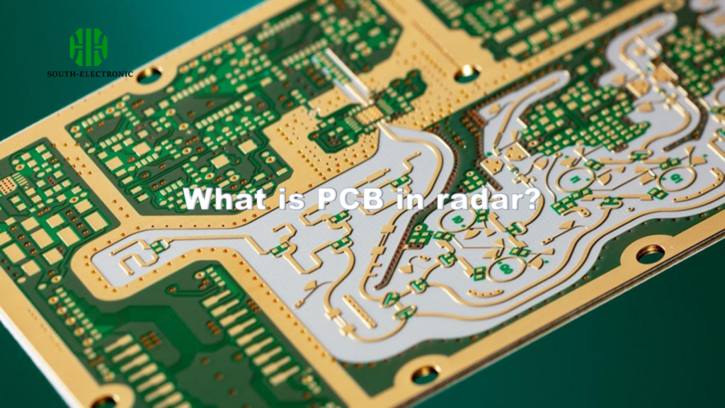
Radar PCBs enable critical detection from storm tracking to touchless devices. Discover innovations in materials, ruggedization & cost reduction driving weather & consumer applications.
How to Identifying Good vs Bad Solder Joints?
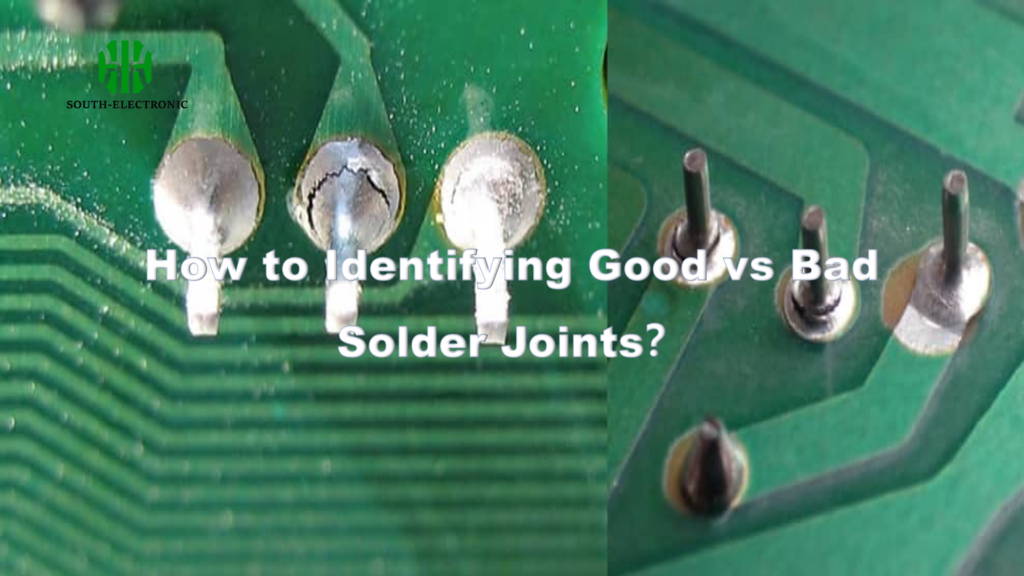
Spot shiny, smooth solder joints; avoid dull, cracked ones. Use correct solder/flux for electronics or plumbing to prevent failures and save costs. Master inspection for reliability.
What is a Via in PCB Design?

Master PCB via design: Choose blind/buried vias for dense layouts, calculate size/spacing to prevent overheating, and avoid common failure causes. Essential for modern circuit reliability.
How to Read Schematic Diagram?
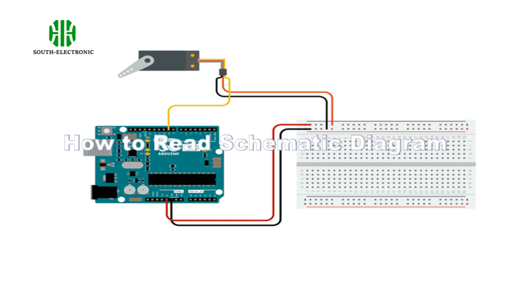
Learn circuit schematic basics: wire connection rules (dots = connected), component symbols like Rs and Cs, and practical debugging steps using diagrams to avoid wiring disasters.

