
What are the differences between FPC, PCB and SMT?
Essential guide to SMT workshop operations: PCB/FPC materials, environmental controls (temp/humidity), solder paste handling, process flow, ESD protection, quality systems & standards for efficient electronic assembly.
PCB board thickness classification and how to choose? Choose the right one and save tens of millions of costs!
PCB thickness (0.3-4.0mm) impacts mechanical strength, thermal performance, signal integrity, & cost. Standard is 1.6mm. Choose ultra-thin (0.2-0.8mm), thick (2.4-3.2mm), or standard based on application & budget.
FPC flexible PCB processing technology knowledge
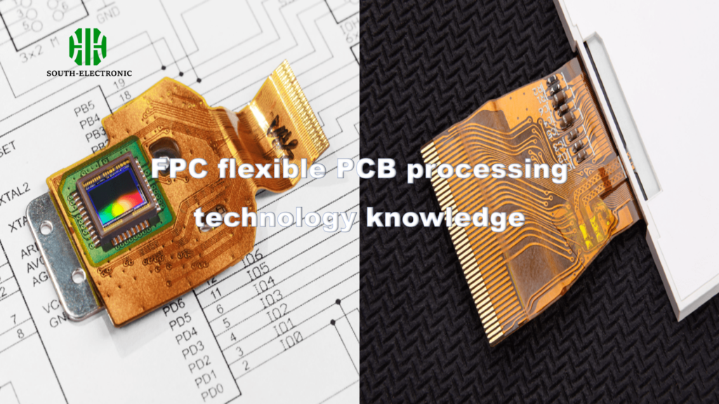
FPC flexible printed circuit boards are vital in electronics, classified as single/double-sided or multi-layer. They use key materials like FCCL, cover film, adhesive film, and copper foil, manufactured via sheet-by-sheet or roll-to-roll processing.
Understand the relationship between layout and PCB in one article
Master PCB layout to minimize switching power supply EMI. Key strategies: reduce high di/dt & dv/dt loop areas, implement loop cancellation, optimize grounding schemes, shield noise sources, and partition circuits effectively.
Do you know the basics of PCB component packaging?
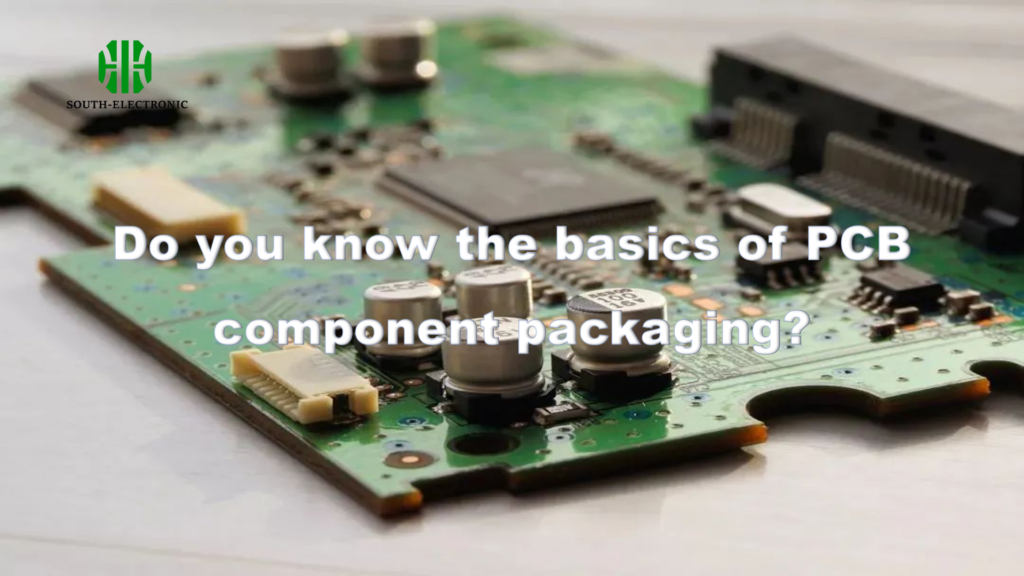
Master PCB component packaging basics: types (DIP plug-in vs. SMD surface mount), common packages for diodes, capacitors, resistors, and ICs, essential elements (pads, outline, silkscreen), and Allegro file suffixes to prevent design errors.
What is PCB Reflow?

Reflow soldering forms critical PCB connections. Learn how temperature control prevents defects like cold joints, component drift & board warping. Optimize profiles with thermal sensors!
What is a Tooling Hole in a PCB?
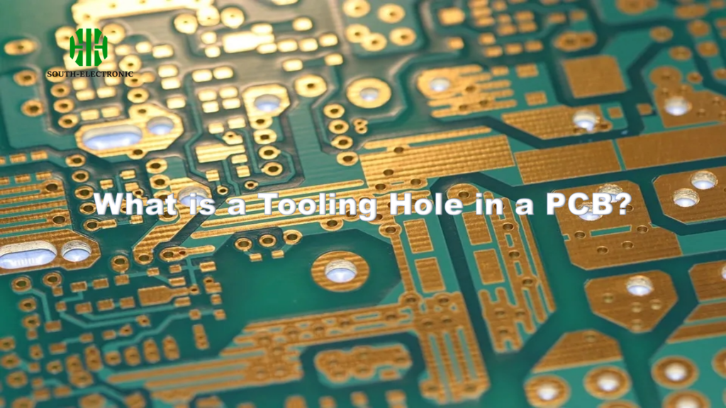
PCB tooling holes are vital for mounting hardware, PCB stability, manufacturing alignment, and test fixtures. Design standards prevent failures; detail is critical for mfg success.
How to master PCB stackup design?
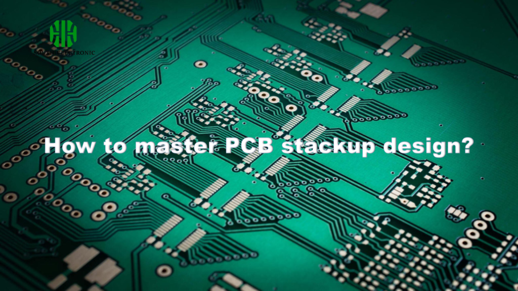
Master PCB stackup design: factors like cost, signal layers, EMI reduction & symmetry. Key principles for impedance control, power-ground coupling & layer arrangement in multilayer boards.
What are the standards for PCB pad design?
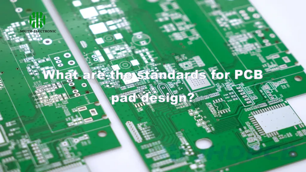
PCB pad design standards prevent defects: min pad size 0.25mm, max 3x aperture, shapes like oval/rectangular. Avoids soldering failures, production delays, scrap costs. Optimizes reliability and efficiency.
What are the reasons for poor etching of PCB boards?
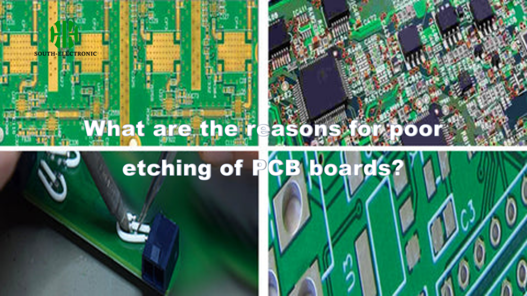
Ensure etching quality in PCB manufacturing to prevent incomplete etching, side etching, etching interlayer, over-etching, and dry film bite. Optimize parameters, maintain equipment, and train staff for high yield and reliability.

