
What is a Burn-in Board?
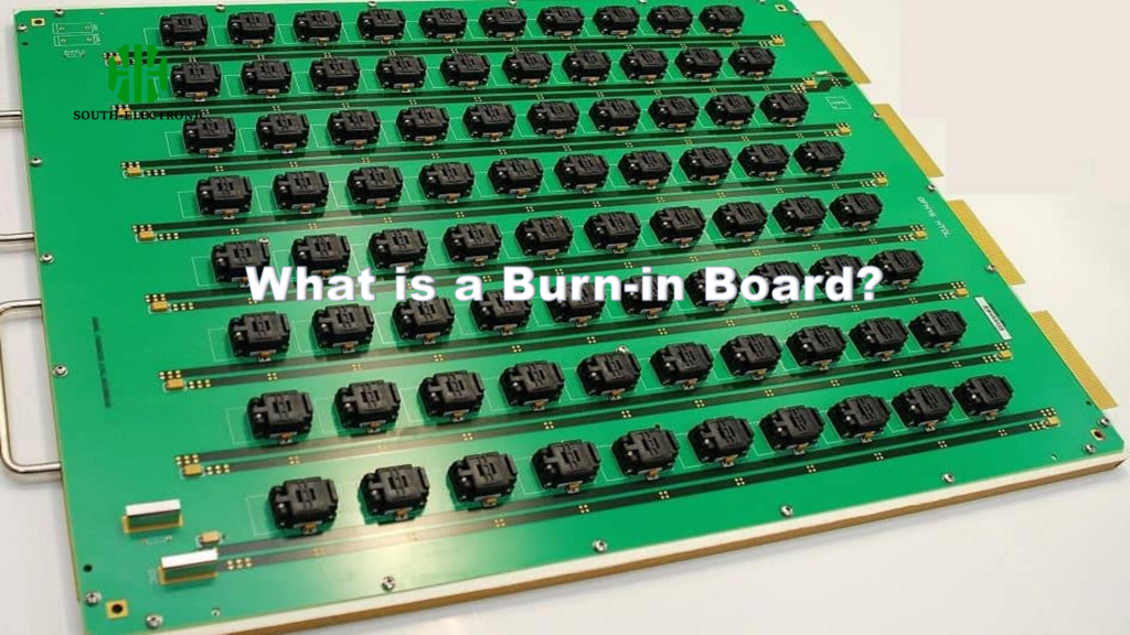
Burn-in boards stress-test semiconductors to ensure reliability, prevent premature failures, and meet auto/medical industry standards.
How to Design the PCB in a Mobile Phone?
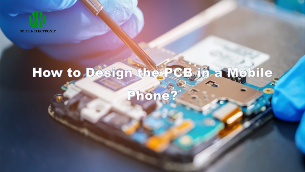
Master smartphone PCB design: HDI layering, thermal vias, signal shielding, military testing for reliability in compact devices.
SMT reflow PCB temperature curve explanation
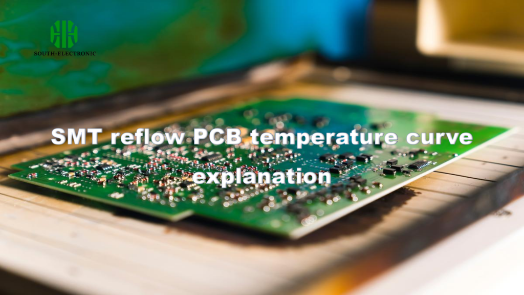
Solder reflow requires precise thermal profiles (preheat, soak, reflow, cooling) with 2-5°C/s ramp rates, 215±5°C peak, and controlled cooling to ensure defect-free metallurgical bonding.
The Difference Between Immersion Gold and Gold Plating in PCB
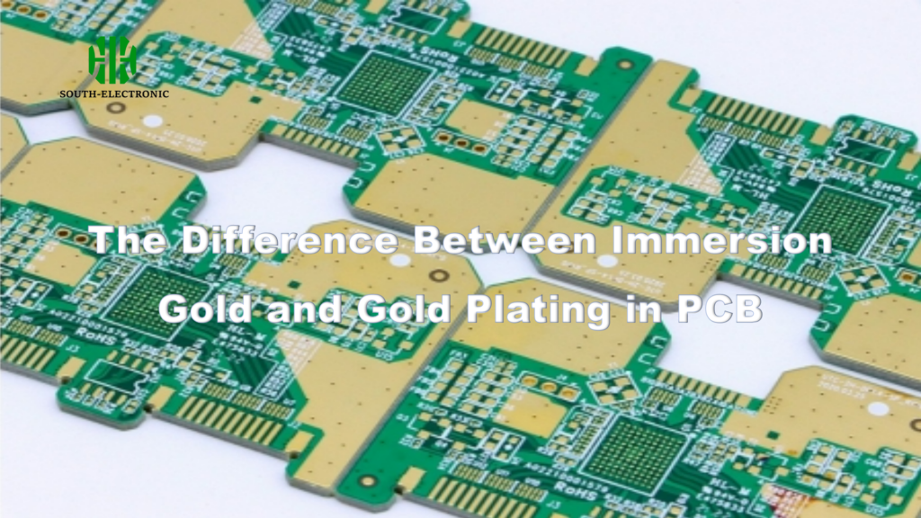
ENIG vs gold plating: ENIG excels in complex/high-frequency PCBs, gold plating for durability. Choose based on cost, conductivity, environment.
What is a Round PCB?
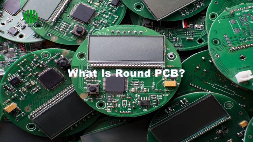
Round PCBs optimize space in compact devices like wearables but face unique design challenges. Learn key considerations for effective implementation.
What Is Zero PCB?
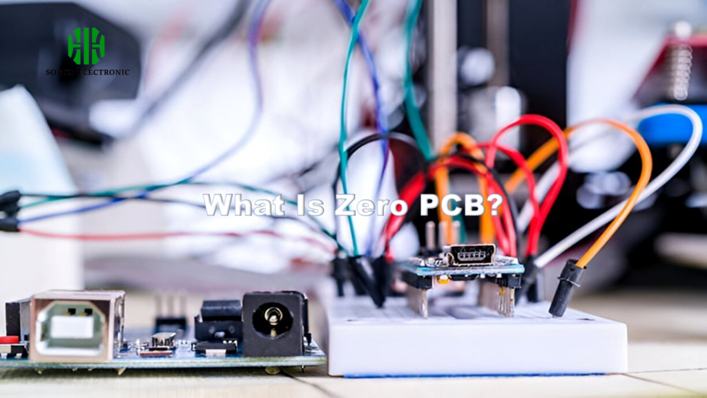
Zero PCB vs. Vero Board: Key differences, ideal uses, and step-by-step soldering tips for efficient DIY electronics prototyping.
What is Wire Bonding?
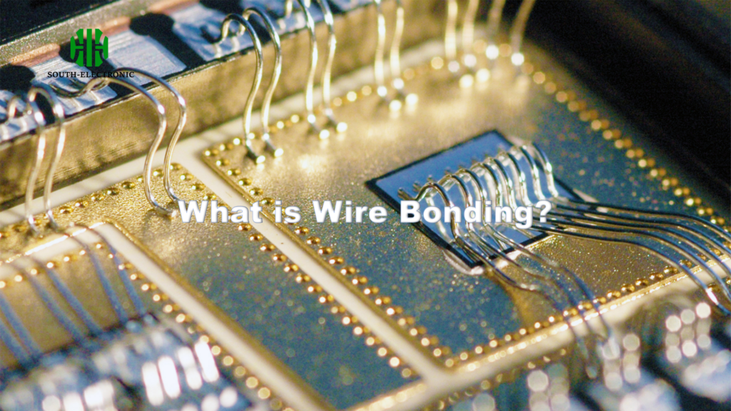
Wire bonding enables precise microchip connections using ultrasonic tech, outperforming soldering in heat-sensitive semiconductor production with unmatched reliability.
What Is a WiFi PCB ?
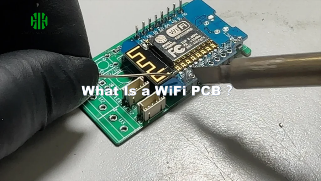
Critical WiFi PCB design: components selection, impedance control, EMI mitigation, material optimization for stable high-speed connectivity.
What Is ENIG Black Pad?
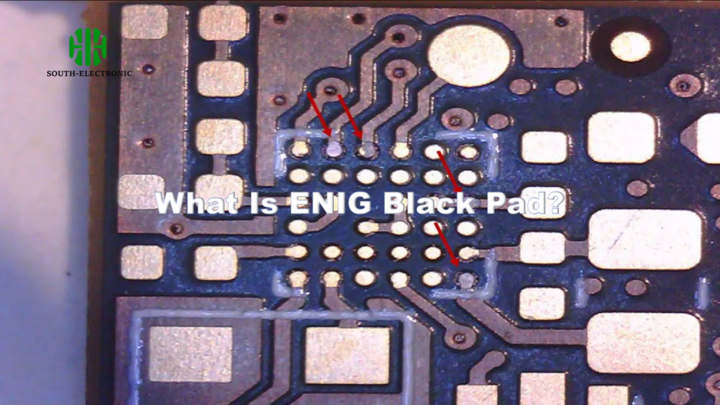
ENIG black pad: Hidden nickel corrosion under gold plating causing PCB failures. Learn causes, detection, prevention prevents costly repairs.
PCB Tombstone: What Is It and How to Avoid It?
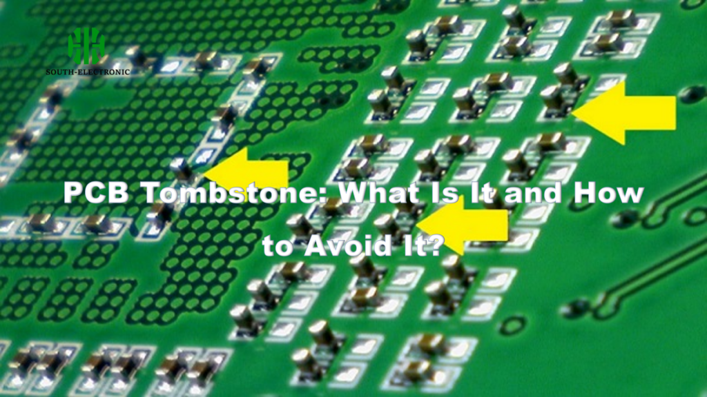
Prevent PCB tombstoning via balanced pad design, precise thermal profiles, and controlled solder paste to neutralize uneven solder forces.

