
Why is Snake-Shaped Routing Necessary on PCB Boards?
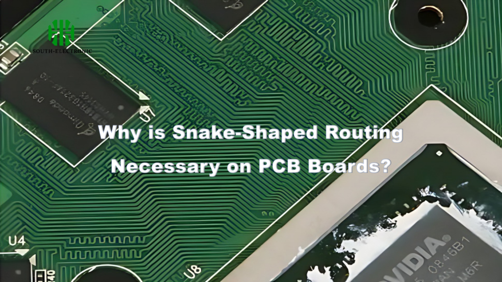
Serpentine routing balances signal delays in high-speed PCB designs using controlled trace bends, solving timing errors while preserving signal integrity. Essential technique.
What is a PCB Simulation?

PCB simulation identifies design flaws early through virtual testing, preventing costly errors and production delays.
Why Is Copper the Go-To Material for PCB Thermal Management?
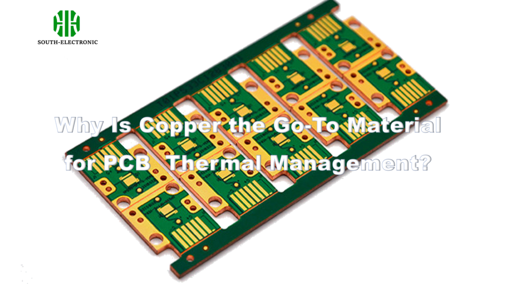
Copper dominates PCBs, balancing 97% of silver’s conductivity at 1/60th cost and 5x aluminum’s thermal efficiency, enabling compact, powerful electronics.
Can You Solder on Tin?
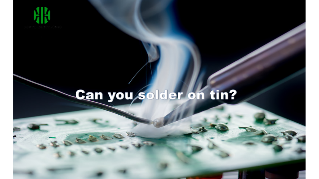
Learn to solder tin safely using temp control, proper flux, and surface prep. Ideal for electronics, crafts, and repairs without melting base materials.
How to Optimiz PCB Stack-up Design?
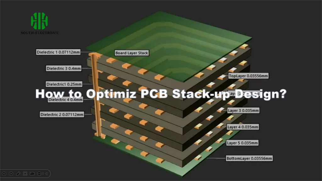
Optimize PCB stack-up with hybrid materials and layer planning. Reduce costs 25-40% while maintaining high-speed signal integrity.
What Materials Are Used in PCB Stackup?
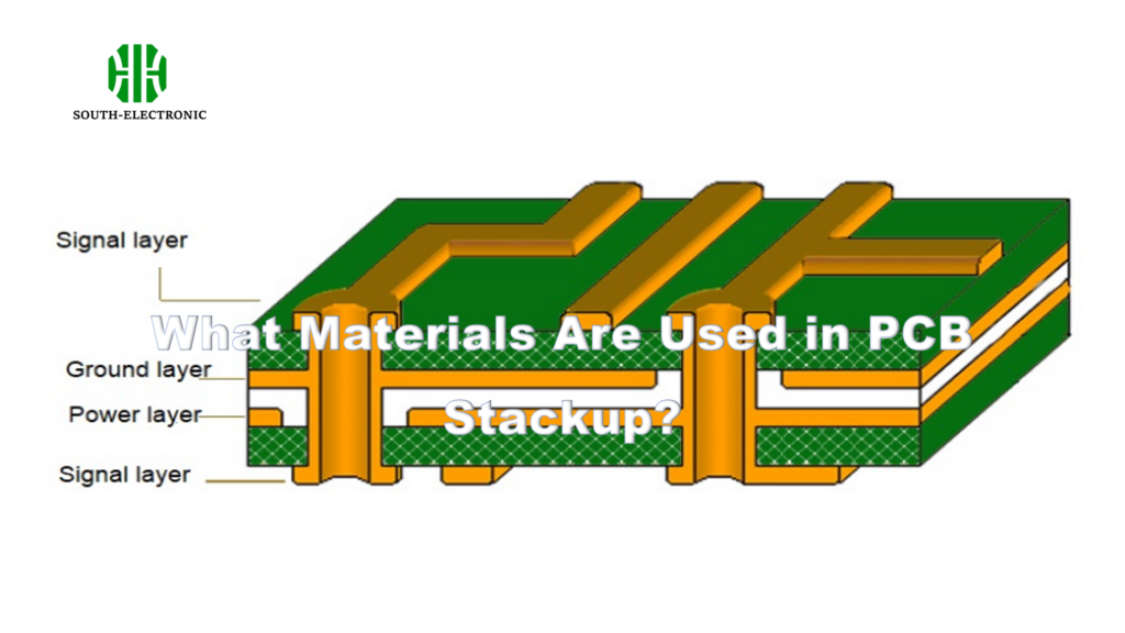
Avoid PCB failures: Learn core vs. prepreg uses, high-speed dielectrics, copper weight impact, and flex material requirements for thermal stability & signal integrity.
Want to Slash PCB Design Costs?
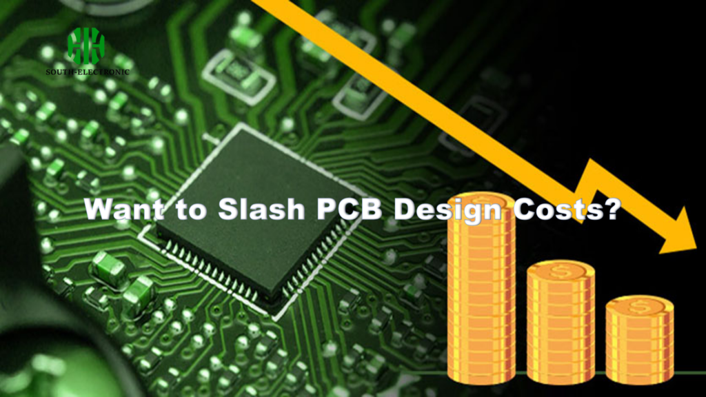
Optimize PCB costs via design-phase planning, strategic layer reduction, and modular architecture – proven methods from hardware prototyping.
What Is Via in Pad?
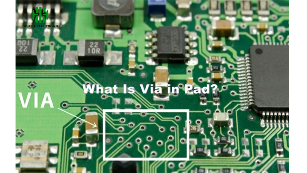
Via-in-pad solves signal distortion in high-speed PCBs, saves space for 5G/IoT designs, but needs thermal care and costs 20-30% more.
Powering the Future: The Evolution of Battery PCB Technology

This article delves into the specialized world of Battery PCBs, essential for managing power in today’s battery-operated devices. From smartphones to electric vehicles, learn how these boards optimize battery life, ensure safety, and enhance efficiency.
What is Copper Thieving in PCB?
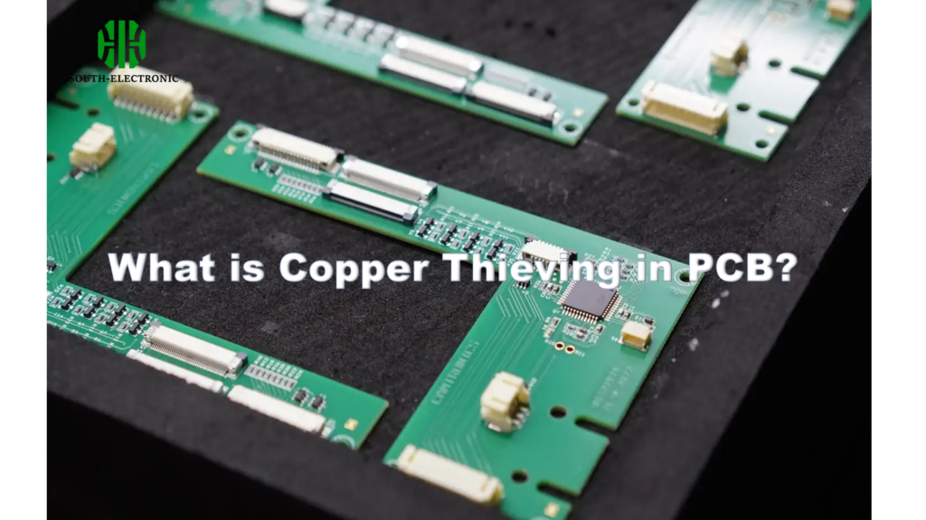
Copper thieving balances PCB fabrication needs & signal integrity – master high-speed impacts, EMI risks, and geometry tradeoffs through physics-driven design.

