
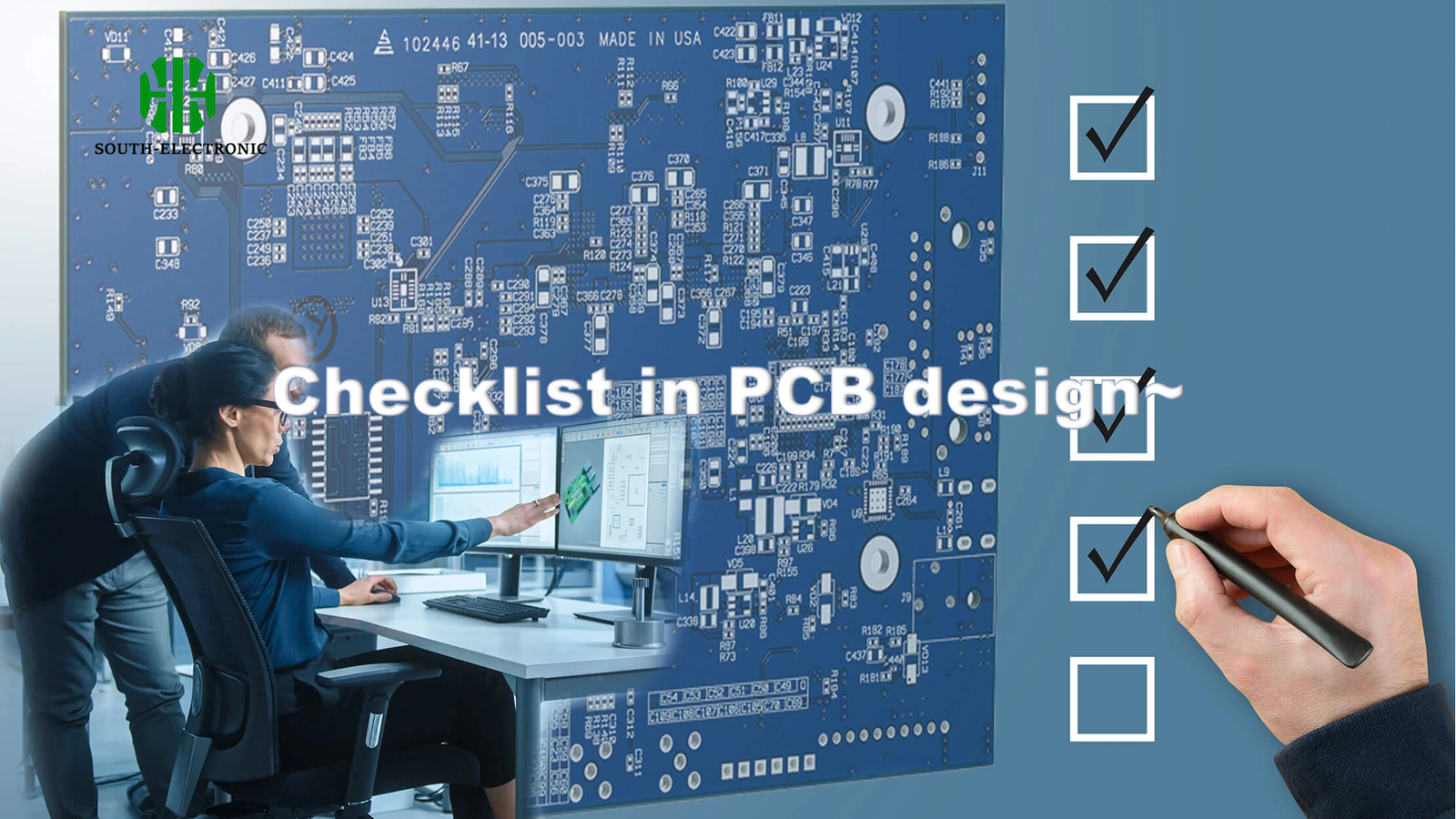
🔧 Data Input Stage Checklist!
- 📋 Document Completeness: Are schematics, *.brd files, BOM, design specs, etc., all received?
- ⏱️ Template Currency: Confirm the PCB template[^1] is the latest version—old templates cause issues!
- ⏰ Clock Device Layout: Check if clock components are placed rationally to avoid signal interference
- 📌 Positioning Devices: Verify positioning device coordinates in the template are 100% accurate
- 📝 Design Requirement Clarity: Ensure design notes, modification requests, and standards are unambiguous
- 🚫 Prohibited Zones: Confirm forbidden placement/routing areas on the outline are mirrored in the template
- 📏 Dimensions & Holes: PCB dimensions, tolerances, and metalized hole definitions must be precise
- 🔒 Template Locking: Lock the structure file after verification to prevent accidental edits

🔍 Post-Layout Inspection: 6 Core Dimensions!
🌟 Component Inspection Essentials
- ✅ Package Consistency: All component packages must match the company library—use viewlog for updates
- 🔄 Board Interfaces: Ensure signal/position correspondence between mother/daughterboards; correct connector orientation with anti-misinsertion designs
- 🧩 100% Placement: Confirm all components are placed—no stragglers!
- 🛑 Overlap DRC Check: Enable TOP/BOTTOM place-bound layers to scan for DRC issues from overlaps
- 🎯 Mark Points: Mark points must be sufficient for production positioning
- ⚖️ Heavy Component Placement: Position heavy components near PCB supports to minimize warping
- 🔒 Structure-Locked Components: Lock structure-related components after layout to prevent displacement
📡 Functional & Signal Integrity Checks
- 📊 Analog/Digital Partitioning: Separate analog/digital circuits on mixed boards with rational signal flow
- ⚡ High-Speed Layout[^2]: Clock/high-speed devices and termination resistors must follow SI guidelines
- 🔗 Reference Plane Treatment: Coupling capacitors for cross-plane signals should be near routing areas
- ⚙️ Decoupling Capacitors: Quantity and placement of IC decoupling caps directly impact signal stability
- 🛡️ EMC Component Placement: EMC-sensitive parts[^3] like reset circuits must follow design guidelines
🔥 Thermal & Power Planning
- 🌡️ Heat-Sensitive Components: Crystals, liquid caps, etc., should stay away from high-power heat sources
- 🔋 Power Path Optimization: IC power supplies must not be too distant; rational LDO/module power layouts
📡 Post-Routing Final Verification: 10 Critical Modules!
⚡ High-Speed & Analog/Digital Routing
- 📶 Impedance Consistency: Maintain uniform impedance for high-speed traces; differential pairs need length matching/symmetry
- ⏱️ Clock Trace Handling: Route clock lines on inner layers; avoid via-dense areas
- 🔢 Analog/Digital Separation: A/D converters straddle partitions; signals don’t cross split zones
🛡️ EMC & Reliability Design
- 🧲 Crystal Protection: Place ground planes under crystals; no traces through component pins
- ⚠️ Routing Taboos: Avoid acute/right angles; adjacent layer signals should route perpendicularly
- 🌐 Ground Plane Treatment: Power/ground planes free of islands/cracks; add shielding vias at splits
🔌 Power/Ground & Process Details
- ⚡ Current Carrying Capacity: Power/ground via count must meet current requirements (1A/mm trace width reference)
- 📏 Prohibited Areas: No traces near metal components/mounting holes; non-metalized hole clearances must comply
- 🖨️ Silkscreen & Coding: Correct component designators/polarity marks; PCB codes in company-standard positions
🧰 Process & Production Readiness
- 🔍 DRC Zero Plan: Enable constraints to scan DRC errors—resolve all critical issues
- 🎯 Optical Alignment Marks: SMT-side marks avoid traces; add marks near BGA components
- 📦 File Completeness: Gerbers, drill files, SMT coordinates, etc., must be complete with standardized naming
📢 Conclusion: 3 Keys to PCB Design Success!
From data input to routing completion, PCB reliability hinges on systematic inspection processes, detail-oriented control, and cross-stage verification awareness. Overlooking any step risks mass-production issues—internalizing this checklist as design habits is key to high-performance, reliable PCBs!
[^1]: Understanding the significance of the latest PCB templates can help prevent design issues and ensure optimal performance.
[^2]: Exploring high-speed layout techniques can enhance your PCB design, ensuring better signal integrity and performance.
[^3]: Learning about EMC-sensitive part placement can significantly improve your PCB’s reliability and compliance with standards.

