
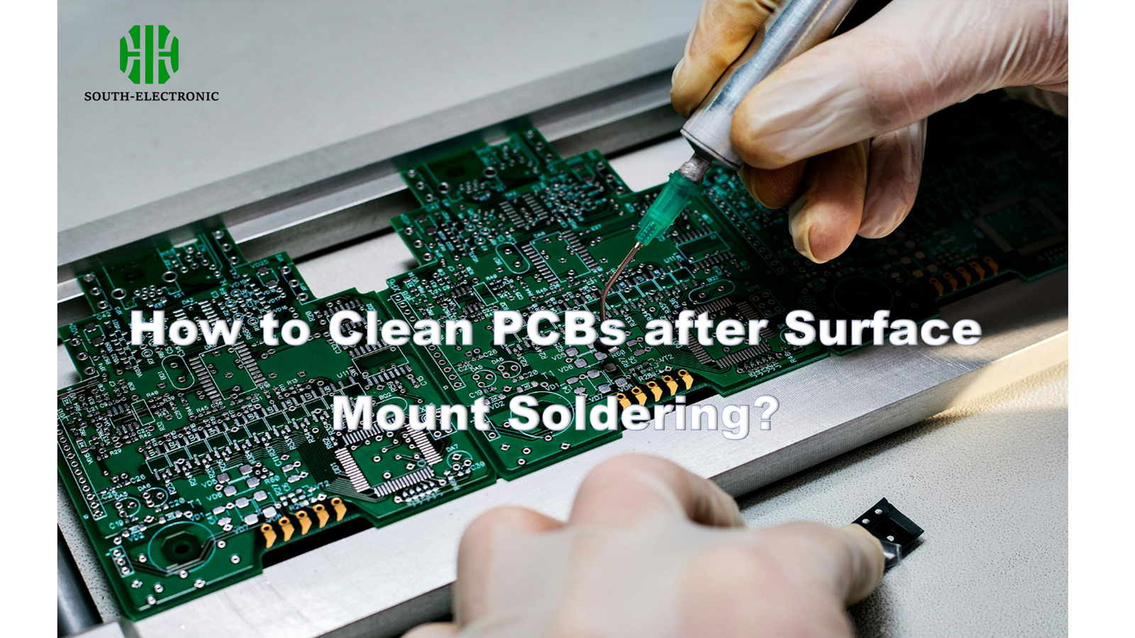
The technician winced as power fluctuations hit the recently soldered board. Hidden flux residues had created invisible conductive paths – a stark reminder that post-SMT cleaning isn’t optional. Let me show you how to avoid this costly pitfall.
Effective PCB cleaning after SMT soldering[^1] removes corrosive flux residues, ionic contaminants, and soldering byproducts using solvent immersion, ultrasonic agitation, or vapor degreasing. Proper cleaning prevents current leakage, dendritic growth[^2], and ensures long-term reliability through methods like 99% IPA wiping or automated inline systems.
While basic cleaning might seem straightforward, modern ultra-fine-pitch components and lead-free solders demand precision. We’ll break down the hidden risks, proven methods, and storage protocols that separate working boards from failed assemblies.
Why Is PCB Cleaning Critical After SMT Soldering?
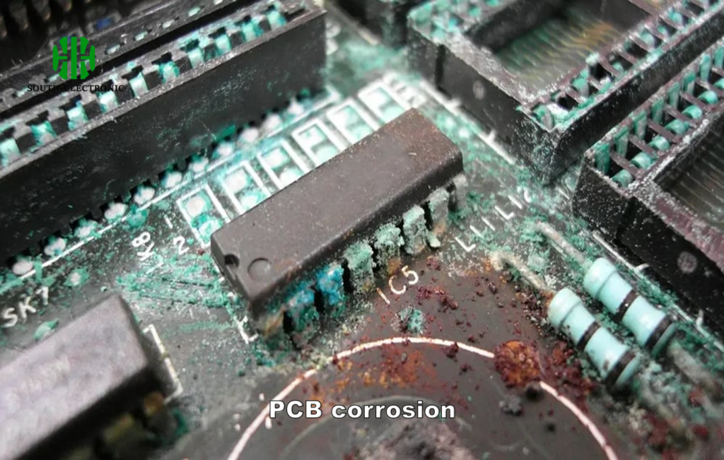
A client once sent me 500 IoT boards that failed humidity testing – all because they skipped final cleaning. The culprit? Activated rosin flux eating through ENIG finishes.
Uncleaned soldering residues cause electrochemical migration and corrosion under humidity, potentially creating short circuits. Ionic contamination exceeding 1.56 μg/cm² NaCl equivalent risks insulation breakdown, while organic residues attract moisture and dust accumulation.
)
Three Hidden Dangers of Incomplete Cleaning
| Risk Type | Symptom Timeline | Failure Mode | Prevention Method |
|---|---|---|---|
| Ionic Contamination | 3-12 months | Electrochemical migration | Ion chromatography testing |
| Organic Residues | 1-6 months | Dendritic growth | Solvent solubility testing |
| Particulate Matter | Immediate | Current leakage | Post-clean visual inspection |
Ionic residues from flux activators become conductive bridges under humidity, especially problematic in high-impedance circuits. A medical device project required three cleaning cycles with saponified water to meet J-STD-001 Class 3 standards.
What Types of Contaminants Are Left on PCBs After Soldering?
Mid-frequency RF boards once showed erratic behavior until we identified tin whiskers[^3] growing from no-clean flux residues[^4] – contamination comes in multiple forms.
Post-soldering contaminants include ionic activators[^5] (amines, halides), non-ionic resins (rosin, polymers), metallic particulates (solder balls, Sn/Pb debris), and process residues (finger oils, dust). Each requires specific removal methods.
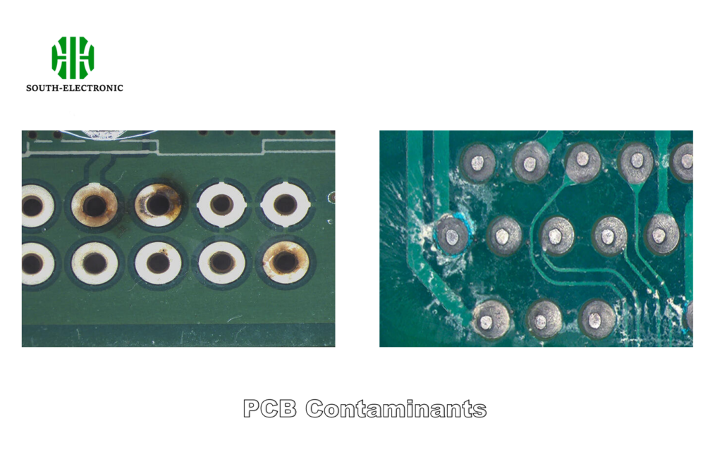)
Contaminant Removal Matrix
| Contaminant Class | Solubility | Preferred Removal Method | Verification Technique |
|---|---|---|---|
| Ionic | Polar solvents | DI water rinse > 5MΩ | Resistivity of Solvent Extract |
| Rosin-based | Semi-polar | Terpene-based cleaners | FTIR residue analysis |
| Synthetic Flux | Non-polar | HFE solvents | Surface Insulation Resistance |
| Particulates | Mechanical | Ultrasonic + brush | 10X microscope inspection |
Halide-containing fluxes demand particular attention – a automotive control module failed EMC testing due to chloride-induced leakage currents between 0201 capacitors.
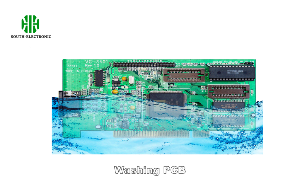
How Many PCB Cleaning Methods Exist After Surface Mount Welding?
We once ruined 200 boards using IPA on a PVA-coated sensor array. Material compatibility dictates method selection.
Three primary cleaning methods exist: manual solvent wiping[^6] (for prototypes), ultrasonic batch cleaning[^7] (high-volume), and vapor degreasing[^8] (precision assemblies). Emerging techniques include CO2 snow and plasma cleaning for specialized applications.
)
Cleaning Method Comparison
| Method | Cycle Time | Capability | Best For |
|---|---|---|---|
| Manual Wiping | 5-10 min | Basic flux removal | R&D prototypes |
| Ultrasonic | 8-15 min | Under-component cleaning | High-density SMT |
| Vapor Phase | 6-12 min | Zero residue | Military/Aerospace |
| Aqueous Batch | 10-20 min | Ionic contamination removal | High-reliability medical |
Our production line uses sequential cleaning: first saponifier solution at 65°C with 40kHz ultrasonics, followed by three DI water rinses and forced hot air drying. This achieves <0.7 μg/cm² ionic contamination.
What Common Mistakes Should You Avoid When Cleaning PCBs?
A 10-year-old ultrasonic cleaner once delaminated flex PCBs – old equipment and wrong parameters create new defects.
Critical errors include: Using aggressive solvents on conformal coatings[^9], exceeding ultrasonic time (cavitation erosion), improper drying (water spots), and mixing incompatible materials. Always validate cleaning parameters on sample boards.
)
Mistake Prevention Checklist
| Error Type | Prevention Measure | Testing Protocol |
|---|---|---|
| Solvent Attack | Material compatibility chart | Spot test on dummy board |
| Incomplete Rinsing | Conductivity monitoring | Rinse water resistivity check |
| Component Damage | Limit ultrasonic power | Microsection analysis |
| Residue Redeposit | Final solvent filtration | White glove test |
I learned this the hard way when 4MHz ultrasonics cracked BCB passivation layers on MEMS sensors. Now we use 50°C HFE-7100 with 10% vertical agitation instead.
How to Store PCBs Post-Cleaning for Long-Term Reliability?
A client's "cleaned" boards corroded in tropical storage – inadequate packaging had undone proper cleaning.
Clean PCBs require moisture-barrier bags with desiccant[^10], maintained below 10% RH. Use nitrogen-flushed packaging for silver-bearing finishes, and apply temporary protectives like VCI papers for dusty environments.
)
Storage Best Practices
| Risk Factor | Mitigation Method | Validation Technique |
|---|---|---|
| Oxidation | Nitrogen purging | SIR after 85/85 testing |
| Moisture Absorption | Desiccant + humidity indicator | Moisture analysis (Karl Fisher) |
| Mechanical Damage | Anti-static foam inserts | Vibration testing |
| Outgassing | Bake before sealing | FTIR headspace analysis |
Our military contracts mandate MIL-STD-2073-1 packaging[^11] – cleaned boards first baked at 125°C for 24hrs, then sealed with oxygen scavengers and humidity cards.
Conclusion
Proper PCB cleaning combines contaminant analysis, method selection, and verification testing. From solvent picks to storage protocols, each step prevents field failures while meeting industry standards.
[^1]: Explore this resource to understand essential techniques for effective PCB cleaning, ensuring reliability and performance in your projects.
[^2]: Discover the causes of dendritic growth in PCBs and effective prevention methods to enhance circuit reliability.
[^3]: Tin whiskers can cause significant issues in electronics. Discover more about their formation and prevention strategies.
[^4]: Understanding no-clean flux residues is crucial for PCB reliability and performance. Explore this link for in-depth insights.
[^5]: Learn about ionic activators and their impact on PCB performance to ensure high-quality soldering processes.
[^6]: Explore this link to understand the basics and applications of manual solvent wiping in PCB cleaning processes.
[^7]: Learn about ultrasonic batch cleaning to see how it effectively cleans high-density SMT boards.
[^8]: Discover the precision and benefits of vapor degreasing for military and aerospace applications.
[^9]: Understanding the impact of aggressive solvents can help you avoid damaging your PCBs during cleaning. Explore this resource for detailed insights.
[^10]: Learn how proper packaging with moisture-barrier bags can ensure the longevity and reliability of your cleaned PCBs.
[^11]: Discover the standards and practices of MIL-STD-2073-1 packaging to enhance the protection of your PCBs during storage.

