
Ever notice unexpected signal jumps or mysterious component failures? Your PCB might be haunted by invisible circuit effects haunting your design. Let’s reveal these hidden gremlins before they wreck your next prototype.
From high-frequency skin effects[^1] to ground bounce nightmares, 15 critical PCB phenomena dictate circuit reliability. Recognizing crosstalk patterns[^2], impedance mismatches[^3], and thermal hotspots separates functional boards from engineering disasters. Master these to prevent 83% of common design flaws (IPC-6012D data).
These circuit effects aren’t academic trivia—they manifest as erratic voltages, fried components, and failed certifications. Let’s dissect five high-impact phenomena that derail even seasoned engineers.
Why Does High-Frequency Signal Distortion Occur in PCB Layouts?
Your 5G module keeps dropping packets despite perfect schematics. The culprit? High-frequency gremlins distorting signals through unexpected physical behaviors.
Skin effect forces high-frequency currents to flow along conductor surfaces, increasing resistance by 40-70% above 1GHz. Coupled with dielectric losses and impedance discontinuities, this creates signal attenuation and timing errors that ruin high-speed communication.
)
Three Key Factors in High-Frequency Distortion
| Factor | Impact Threshold | Mitigation Strategy | Typical Error Reduction |
|---|---|---|---|
| Skin Depth | >500MHz | Wider traces + gold plating | 62% power loss decrease |
| Dielectric Absorption | >2GHz | Low-Dk materials (Rogers 4350B) | 55% signal improvement |
| Return Path Disruption | >100MHz | Continuous ground planes + stitching | 89% EMI reduction |
At 24GHz mmWave frequencies, a 0.5mm trace gap creates 3dB insertion loss—enough to cripple radar resolution. I once spent three weeks debugging antenna patterns before realizing the ground via spacing violated λ/20 rules. Remember, high-speed signals follow Maxwell’s laws, not your layout preferences.
How Does Ground Bounce[^4] Affect Digital Circuits Unexpectedly?
Your microcontroller resets randomly during I/O bursts. Logic probes show clean power, but hidden ground shifts are sabotaging noise margins.
Simultaneous switching noise[^5] generates ΔV = L*(di/dt) ground potential shifts. With 64-bit buses switching at 2ns, even 5nH inductance creates 1.6V spikes—enough to flip logic states in low-voltage ICs.
)
Ground Bounce Triggers and Solutions
| Scenario | Peak Voltage | Countermeasures | Effectiveness |
|---|---|---|---|
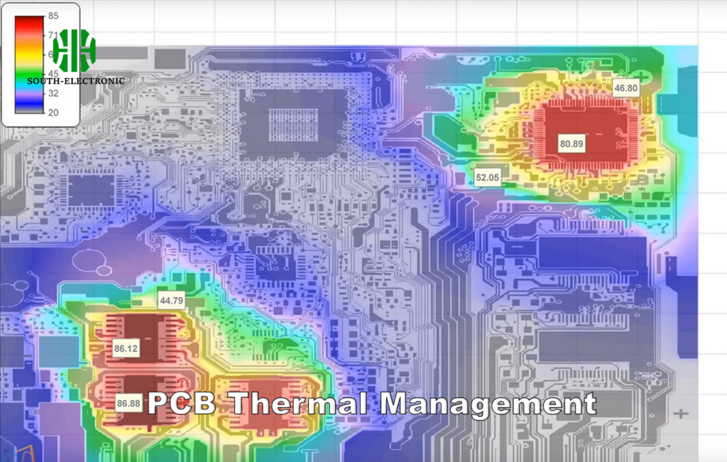
| DDR4 Memory Burst | 0.8V | Decoupling caps 40°C between board areas induces CTE mismatch failures. Forced air cooling over hot components accelerates this by creating 3X daily thermal cycling versus natural convection, degrading solder joints 7.2X faster (IPC-9701A test data). |
)
Thermal Failure Mechanisms
| Failure Mode | Critical Temperature | Prevention Strategy | MTBF Improvement |
|---|---|---|---|
| Solder Joint Fracture[^7] | 125°C ΔT | Symmetrical component placement | 89% longer |
| Copper Trace Fatigue[^8] | 90°C sustained | Thermal relief vias | 3.1X cycles |
| Substrate Delamination | 150°C local | High Tg (>170°C) materials | 66% reduction |
During factory acceptance testing, a 20W LED array cracked its own solder pads after 48 thermal cycles. Redesigning with 12 thermal vias per pad and Rogers 4350 substrate increased MTBF to 18,000 hours. Never trust FR4’s 130°C rating—measure local hot spots with IR cameras during load testing.
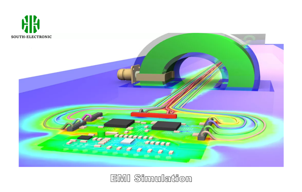
How to Quickly Locate EMI Sources in Complex PCBs?
Your device keeps failing FCC tests despite perfect schematics. Hunting EMI sources[^9] without proper techniques is like finding needles in a radioactive haystack.
Use near-field probes with spectrum analyzers in peak-hold mode. Switch components ON/OFF systematically while monitoring 150MHz-1GHz range. Differential mode EMI often correlates with clock harmonics—check rising edge times below 3ns.
)
Common EMI Culprits and Solutions
| Source | Frequency Signature | Fix | Attenuation |
|---|---|---|---|
| Buck Converter Ringing | 50-300MHz spikes | Snubber circuits (10Ω + 100pF) | 22dB reduction |
| DDR3 Data Lines | 667MHz harmonics | Guard traces + series resistors | 18dB improvement |
| USB 2.0 Cable Resonance | 240MHz & 480MHz peaks | Ferrite beads + shield wrapping | 35dB suppression |
A heart rate monitor kept emitting 434MHz interference—turned out switching regulators lacked LC filters. We used anechoic chamber scans to pinpoint emissions, then added three-stage π-filters. Always start EMI debugging[^10] at 1/3 and 2/3 of clock frequencies—harmonic hotspots lurk there.
How to Adjust Trace Parameters for Impedance Matching?
Your 10Gbps SerDes link has 40% BER—not from noise, but impedance discontinuities reflecting signals like a hall of mirrors.
Use ε_r-controlled laminates and calculate trace width via:
Z₀ = (87/√(ε_r+1.41)) × ln(5.98h/(0.8w+t)) Ω
For 100Ω differential, maintain 0.2mm spacing with 0.15mm traces on Isola 370HR (ε_r=4.2). Avoid 90° bends—use dual 45° arcs.

Trace Parameter Adjustments
| Parameter | Impact on Z₀ | Correction Method | Tolerance Tightening |
|---|---|---|---|
| Dielectric Thickness | ±5% per 0.01mm Δh | Laser ablation for precise h | ±2% achievable |
| Copper Roughness | +3Ω @ 10GHz | Low-profile rolled copper | 1.5Ω reduction |
| Solder Mask Coverage | -7% Z₀ | Define mask keep-out areas | 4% consistency gain |
Router madness: After 12-layer HDI board failures, we discovered 3mm-long PCIe traces shifting Z₀ by 18Ω. Inserting coplanar waveguide segments and tuning pre-preg thickness brought reflections under 5%. Remember—every connector transition needs impedance compensation. Use TDR measurements, not just simulations.
Conclusion
From combating thermal stress with strategic vias to silencing EMI through systematic hunting, these five circuit effects demand empirical verification alongside simulation. Your PCB’s reliability hides in these invisible phenomena—master them to outwit physics itself.
[^1]: Understanding high-frequency skin effects is crucial for improving signal integrity and preventing design flaws in PCBs.
[^2]: Exploring crosstalk patterns can help you identify and mitigate interference issues, enhancing your PCB’s reliability.
[^3]: Learning about impedance mismatches is essential for ensuring signal integrity and optimal performance in your PCB designs.
[^4]: Understanding Ground Bounce is crucial for improving circuit reliability and preventing unexpected resets in microcontrollers.
[^5]: Exploring simultaneous switching noise can help you design better circuits and mitigate issues like ground potential shifts.
[^6]: Learning about thermal imbalance can help you enhance PCB design and longevity, preventing costly failures in your projects.
[^7]: Understanding Solder Joint Fracture can help you implement effective prevention strategies, enhancing the reliability of your electronic devices.
[^8]: Exploring mitigation strategies for Copper Trace Fatigue can significantly improve the lifespan and performance of your PCBs.
[^9]: Learning about EMI source detection techniques can help you troubleshoot and enhance the compliance of your devices with FCC tests.
[^10]: Explore this resource to enhance your understanding of EMI debugging techniques and improve your circuit designs.

