
Consumer Electronics PCB Supplier
South-Electronic
At South-Electronic, we specialize in providing high-quality consumer electronics PCB that ensure durability, superior performance, and seamless integration, making your devices more reliable and efficient.
Discover Unmatched Quality with Our Consumer Electronics PCB
Welcome to South-Electronic, your number one source for consumer electronics PCB. Our products are specifically designed to improve the functionality of everything from personal gadgets to household appliances.
When you choose South-Electronic, you can expect nothing but the best in quality and reliability for your consumer electronics. Our PCB will give your products the consistent, powerful performance they need to stand out from the competition. Let us help you become the leader in your industry.
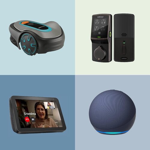
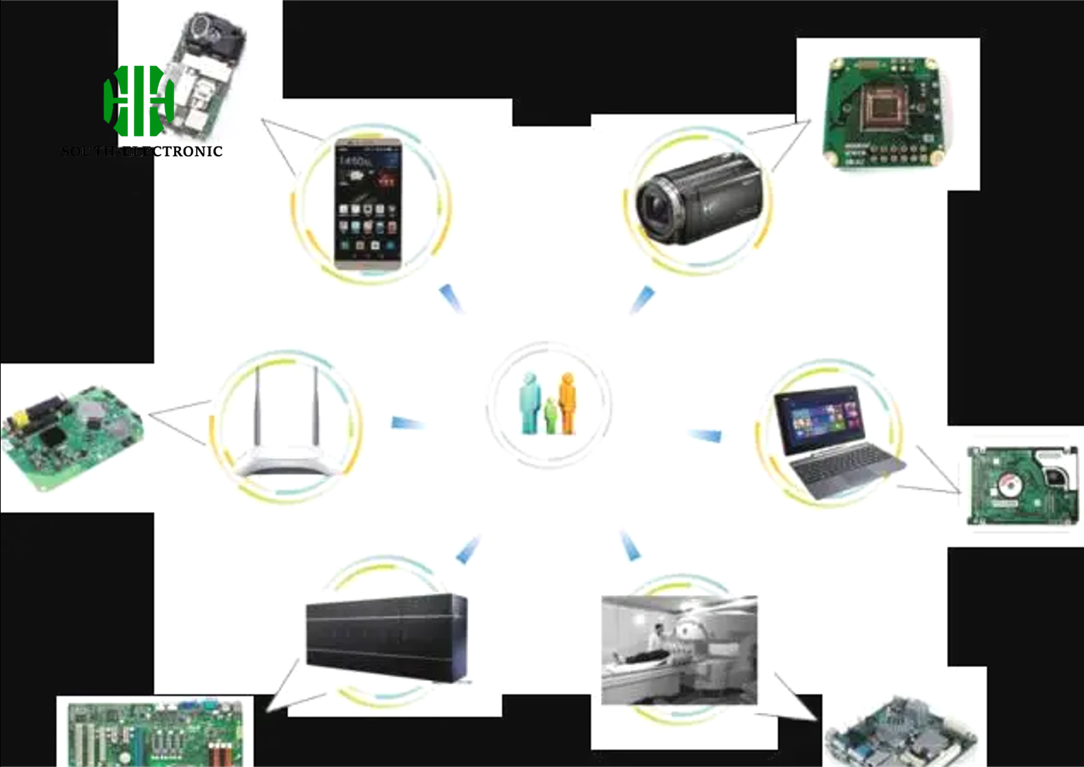
Smart Home Devices
Automated Lighting Systems: Take control of your home lighting with our smart and energy-efficient solutions.
Security and Monitoring Systems: Keep your home safe with our advanced monitoring systems that keep you connected and protected.
Smart Thermostats: Optimize your home's temperature for comfort and savings with our responsive smart thermostats.

Portable Electronics
Smartphones and Tablets: Experience cutting-edge technology and mobility with our high-performance smartphones and tablets.
Portable Music Players: Take your music everywhere with our compact and high-quality portable music players.
E-Readers: Enjoy your favorite books on the go with our lightweight and eye-friendly e-readers.
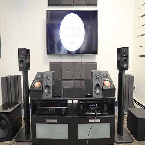
Entertainment System
Gaming Consoles: Dive into immersive gaming with our powerful and versatile gaming consoles.
Smart TVs and Streaming Devices: Stream your favorite shows and movies in stunning clarity with our smart TVs and streaming devices.
Home Theater Systems: Bring the cinema experience home with our state-of-the-art home theater systems.
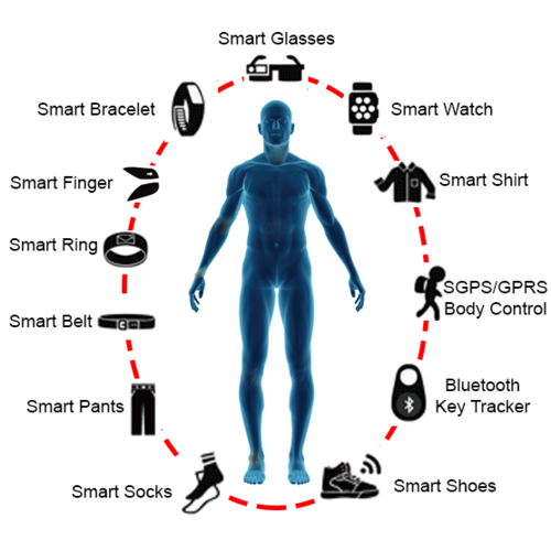
Wearable Technology
Smartwatches: Keep connected, healthy, and punctual with our stylish and functional smartwatches.
Fitness Trackers: Track your fitness goals and progress with our accurate and user-friendly fitness trackers.
VR/AR Headsets: Explore virtual and augmented realities with our innovative VR/AR headsets.

Home Appliances and Kitchen Electronics
Smart Refrigerators: Keep your food fresh longer with our high-tech, energy-efficient smart refrigerators.
Electronic Microwaves: Simplify cooking with our fast and user-friendly electronic microwaves.
Smart Coffee Makers: Brew the perfect cup every time with our programmable smart coffee makers.

Security and Surveillance Systems
Home Security Cameras: Monitor your home remotely with our high-definition security cameras.
Alarm Systems: Protect your property with our reliable and easy-to-set-up alarm systems.
Doorbell Cameras: See and speak with visitors at your door from anywhere with our smart doorbell cameras.
The Complete Guide For Consumer Electronics PCB
Contents
Chapter 1

Introduction to Consumer Electronics PCB
Overview of PCB in Consumer Electronics
PCB is the backbone of modern consumer electronics. They are the foundation upon which various electronic components are mounted to create complex circuits. In consumer electronics, PCB is used in virtually every device, from smartphones and tablets to televisions and microwaves. The design and quality of a PCB determine the functionality, reliability, and performance of the device.
PCB isa big deal in consumer electronics. It makes the electrical connections for transistors, resistors, capacitors, and other components that let modern devices do their thing. As technology has advanced, consumer electronics PCB have gotten more complex, with multi-layer boards that can support more components in a smaller space. That’s allowed for the development of smarter, more energy-efficient, and feature-rich devices that keep changing the way we live.
Importance of PCB in Modern Consumer Devices
PCB is critical for the performance and durability of consumer electronics. They are meticulously designed to withstand the demands of daily use and the specific conditions under which different devices operate. For instance, a PCB used in a wearable device like a smartwatch must be highly durable and flexible, capable of enduring physical stress and environmental factors such as moisture and temperature variations.
Moreover, the importance of PCB extends beyond just functionality. In the consumer electronics industry, where market competition is fierce, the innovation in PCB design directly contributes to the commercial success of products. Advanced PCB can lead to smaller, faster, and more powerful electronics, appealing to consumers seeking the latest technologies. Additionally, the efficiency of a PCB affects the overall energy consumption of the device, which is a critical factor in compliance with global energy standards and consumer preferences for sustainable products.
In conclusion, PCB is indispensable in the development and enhancement of consumer electronics. They not only ensure that devices operate as intended but also play a significant role in the ongoing innovation and marketability of consumer products. As technology continues to advance, the role of PCB in consumer electronics is expected to grow even more, driving new capabilities in connectivity, performance, and user experience.
Chapter 2
Types of PCB Used in Consumer Electronics
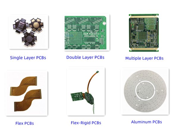
Single-sided, Double-sided, and Multi-layer PCB
Single-sided PCB is the simplest type, they have one layer of conductive material, usually copper, mounted on one side of the board. Components are soldered on one side, and the circuit is printed on the other. These are commonly used in simpler devices such as power supplies, relays, and sensors because they are cheap and easy to make.
Double-sided PCB
have copper layers on both sides of the board, allowing for a higher density of components and interconnections. They are connected by through-holes that pass through the board, providing better flexibility in design. This type is prevalent in more complex devices like LED lighting and automotive dashboards.
Multi-layer PCB
is made up of three or more double-sided boards stacked together. These layers are separated by insulating materials and connected with plated through-holes. Multilayer PCB is essential for modern consumer electronics like smartphones, laptops, and medical devices because they enable enhanced functionality and high-speed signal processing within compact form factors.
Flexible and Rigid-Flex PCB
Flexible PCB is made from materials that can flex and bend, typically using plastic like polyimide or similar polymers. The PCB is lightweight, thin, and can withstand more bending and movement than rigid PCB. They are ideal for modern portable electronics, such as wearable devices, where flexibility and space constraints are a major concern.
Rigid-Flex PCB is a combination of rigid and flexible PCB. They have multiple layers that include both rigid and flexible substrates, which are laminated together to form a single structure. Rigid-flex PCB is used in advanced consumer electronics where complex configurations are required, such as in cameras, cell phones, and high-end wearables. They allow for a more streamlined design by eliminating the need for multiple connectors and interconnecting cables. This improves reliability and performance by reducing the number of solder joints and connectivity issues.
Applications of Different PCB Types
Every type of PCB has a specific use in consumer electronics based on what the device does, how it’s designed, and how long it needs to last:
- Single-sided PCB is often used in light consumer electronics where complexity and costs need to be minimized.
- Double-sided PCB is good for moderately complex devices that need more circuitry than what single-sided boards can provide but at a lower cost than multi-layer boards.
- Multi-layer PCB is necessary for high-performance and multi-functional devices where space and efficiency are important.
- Flexible PCB is commonly found in modern wearables and mobile devices that take advantage of their flexibility and durability to handle movement.
- Rigid-Flex PCB is particularly valuable in applications that demand the durability of rigid boards with the versatility of flexible boards, offering optimal solutions for compact and complex electronic assemblies.
Knowing the different types of PCB and what they’re used for will help you pick the right board for your consumer electronics product. That way, you get the best performance for the least amount of money.
Chapter 3
Materials and Components
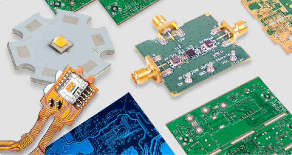
Common Materials Used in Consumer Electronics PCB
The materials you choose are kind of a big deal. They can affect everything from the performance and durability of your board to how easy it is to solder together. Here are some of the most common materials used in consumer electronics PCBs:
Substrate Materials: The base material of a PCB, usually made of fiberglass, known as FR4. FR4 offers excellent electrical insulation and durability at a relatively low cost, making it the standard for many consumer electronics. For high-frequency applications, materials such as Rogers or Teflon are used due to their superior high-frequency performance.
Conductive Layers: Copper is the most common conductive material used for creating the circuitry on PCB. It is chosen for its excellent electrical conductivity and ability to etch fine details. The thickness of the copper layer can vary depending on the application, with higher currents requiring thicker copper.
Solder Mask: This layer is applied over the copper layer to insulate the copper traces and prevent accidental contact with other metal, solder, or conductive bits. This layer helps in avoiding short circuits. It’s typically green but can be applied in different colors for coding or branding purposes.
Silkscreen: Typically white, but available in various colors, this layer is used to add labels and indicators to a PCB, which help in identifying the various components and their orientations.
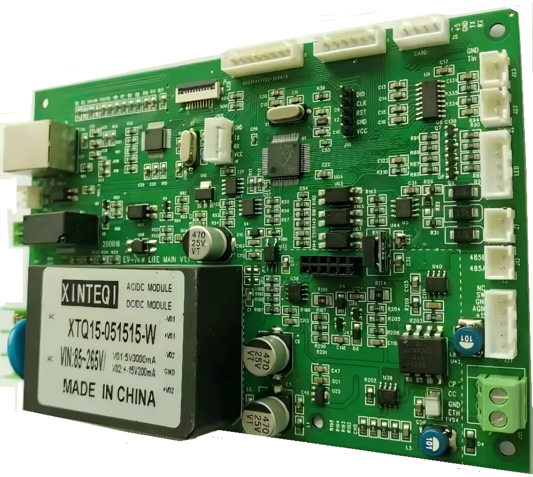
Key Components and Their Roles
PCB contain a variety of electronic components, each with specific functions that are necessary for consumer electronic devices to work:
Capacitors: These components store electrical energy and release it when needed. They are used to smooth out electrical fluctuations, filter signals, and perform timing functions. In consumer electronics, capacitors are crucial for power management and signal integrity.
Resistors: Resistors control the electric current flowing through them. They are used to manage voltage levels within circuits, divide voltages, limit current, and offer load to circuits. Their precise control over current makes them indispensable in nearly all electronic devices.
Integrated Circuits (ICs): Also known as microchips, these components are complex circuits that contain hundreds to millions of transistors, resistors, and capacitors in a tiny package. ICs can function as amplifiers, microprocessors, memory devices, and more. They are the heart of modern electronics, enabling the complex computations and functionalities of consumer devices like smartphones and computers.
Transistors: These are used to switch electronic signals and power. They are the fundamental building block in ICs and are used extensively in amplification and switching applications.
Diodes: Including LEDs, diodes allow current to flow in one direction but block it in the opposite direction. They are used for power conversion, signal demodulation, and regulating voltage levels.
Chapter4
Design Considerations for Consumer Electronics PCB
Designing for Efficiency and Reliability
When it comes to PCB design for consumer electronics, efficiency and reliability are key. Designers need to make sure that each PCB not only meets the functional requirements of the device, but also operates efficiently under different conditions. Here are some key strategies to keep in mind:
Minimizing Power Consumption: When you design circuits that use less power, you extend the battery life of your device and reduce the amount of heat it generates. This means using components that run on less power and building power-saving modes into your device design.
Maximizing Circuit Efficiency: Using the latest design software and simulation tools to optimize the layout and routing of circuits. This means putting components in the right places to make sure critical signals don’t have to travel too far, and using clever routing techniques to reduce interference and signal degradation.
Enhancing Reliability:
Building in redundancy for critical operations, and using quality components known for their long life and solid performance. It also means testing the hell out of things during the design phase to find and fix any weak spots.
Considerations for Compact and Complex Devices
With consumer electronics getting smaller and more powerful, PCB design has to keep up with the compact and complex requirements.
High-Density Interconnect (HDI) Technology: HDI boards have finer spaces and lines, smaller vias, and higher connection pad density than traditional PCB, which supports more functions per unit area, crucial for compact devices like smartphones.
Layer Management:
Effectively using multi-layer configurations to fit more circuitry into limited spaces. This includes planning for the density of the interconnects and making sure all the layers line up and connect without getting in each other’s way.
Component Placement: Strategic placement of components to maximize space, reduce interference, and enhance the overall aesthetic and functional integration within the device.
Thermal Management in PCB Design
Effective thermal management is essential to maintain the performance, reliability, and safety of consumer electronics. Excess heat can lead to device failure, reduced lifespan, and in extreme cases, safety hazards. Key considerations include:
Heat Dissipation Techniques: Incorporating features such as thermal vias, heat sinks, and thermal pads in areas where heat generation is significant. These components help to transfer heat away from sensitive parts of the PCB to areas where it can be more safely dissipated.
Material Choices: Selecting substrates and conductive materials that can withstand higher temperatures and efficiently dissipate heat. Materials like aluminum and copper have good thermal conductivity and are often used in heat-critical applications.
Component Selection and Layout: Choosing components that generate less heat and optimizing their layout to facilitate airflow and heat distribution across the PCB. This includes avoiding clustering high-power components together unless thermally managed.
Simulation and Testing: Using thermal simulation software to predict how heat will be generated and dissipated within the PCB layout, followed by rigorous testing under various operational conditions to ensure thermal stability.
By keeping these design considerations in mind, you can make sure that your consumer electronics PCBs are not only functional and compact, but also safe and reliable for the people who use them. This is how you keep up with the fast pace of innovation and keep your customers happy.
Chapter 5

Manufacturing Processes
Step-by-Step Guide on the PCB Manufacturing Process
The manufacturing of PCB is a complex process that involves several critical steps. Each stage is crucial for ensuring the quality and functionality of the final product. Here’s a detailed look at these steps:
Design and Output: The PCB design is finalized using computer-aided design (CAD) software, which generates detailed layout data. This data is then used to create a production file that guides the manufacturing process.
Material Selection: Based on the application requirements, appropriate substrate and copper materials are chosen. Commonly, materials such as FR4 or polyimide are selected for their durability and electrical properties.
Photoresist Application and UV Exposure: A photoresist layer is applied to the copper layers of the board. The PCB layout is then printed onto a photomask which is used to expose the photoresist under UV light. This develops the image of the circuit pattern on the PCB.
Etching: The areas of the copper not protected by the photoresist are then chemically etched away, leaving behind the pattern of the circuit.
Layering and Bonding: For multi-layer PCB, individual layers are aligned and bonded together under heat and pressure. This process involves the use of prepreg material (a type of bonding glue) to ensure the layers adhere properly.
Drilling: Holes are drilled into the PCB to accommodate through-hole components and to provide vias for inter-layer connections. The precision of drilling is crucial for the functionality of multi-layer PCB.
Plating: The drilled holes are plated with copper to establish a connection between the different layers of the PCB. This plating also strengthens the holes.
Solder Mask Application: A solder mask layer is applied over the entire PCB to protect the copper circuits and prevent short circuits during soldering. This layer also provides the PCB its characteristic green color, although other colors can be used.
Silkscreen Printing: Critical information, such as component labels and test points, is printed on the solder mask layer to facilitate the assembly and maintenance of the PCB.
Surface Finish Application: A surface finish is applied to the copper tracks exposed by the solder mask to protect them from oxidation and to improve solderability during component assembly.
Testing and Quality Control: The completed PCB undergo rigorous testing to check for any potential faults. Techniques like Automated Optical Inspection (AOI), X-ray inspection, and electrical testing are commonly used.
Cutting and Packaging: Finally, the PCB is cut out from the larger panel they were manufactured in and packaged for shipping.
Surface Finish Options and Their Benefits
The choice of surface finish plays a crucial role in the performance and longevity of a PCB. Here are some common surface finish types and their benefits:
HASL (Hot Air Solder Leveling): This is one of the most common and least expensive finishes. It provides good solderability and a long shelf life. However, it’s less suitable for fine-pitch components due to uneven surfaces.
ENIG (Electroless Nickel Immersion Gold): ENIG provides a flat surface and excellent solderability, making it ideal for high-density component layouts. It also offers good corrosion resistance and is lead-free.
OSP (Organic Solderability Preservatives): OSP is a surface finish that provides a flat surface and is good for fine-pitch components. It is environmentally friendly and cost-effective but has a shorter shelf life compared to other finishes.
Immersion Silver: This finish provides excellent solderability and a flat surface. It has a moderate shelf life and is sensitive to handling, as tarnishing can occur if not handled properly.
Immersion Tin: Known for its excellent solderability and good shelf life, immersion tin is also cost-effective. However, it can be susceptible to whisker growth, which can cause electrical shorts.
Chapter 6
Testing and Quality Assurance
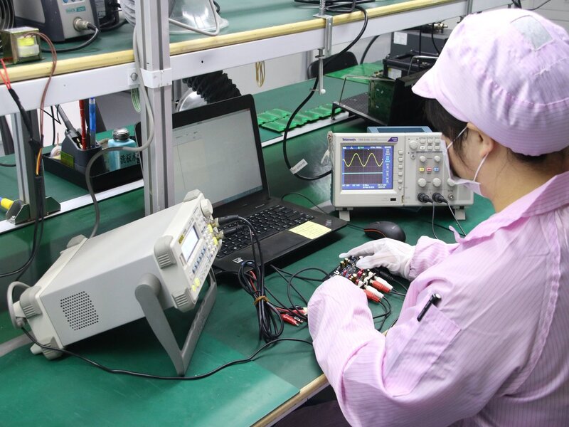
Quality Control Measures and Testing Methods
Quality control in PCB manufacturing is crucial to ensure that the final products meet all specifications and are free from defects that could affect functionality or durability. Here’s an overview of the key quality control measures and testing methods used in the industry:
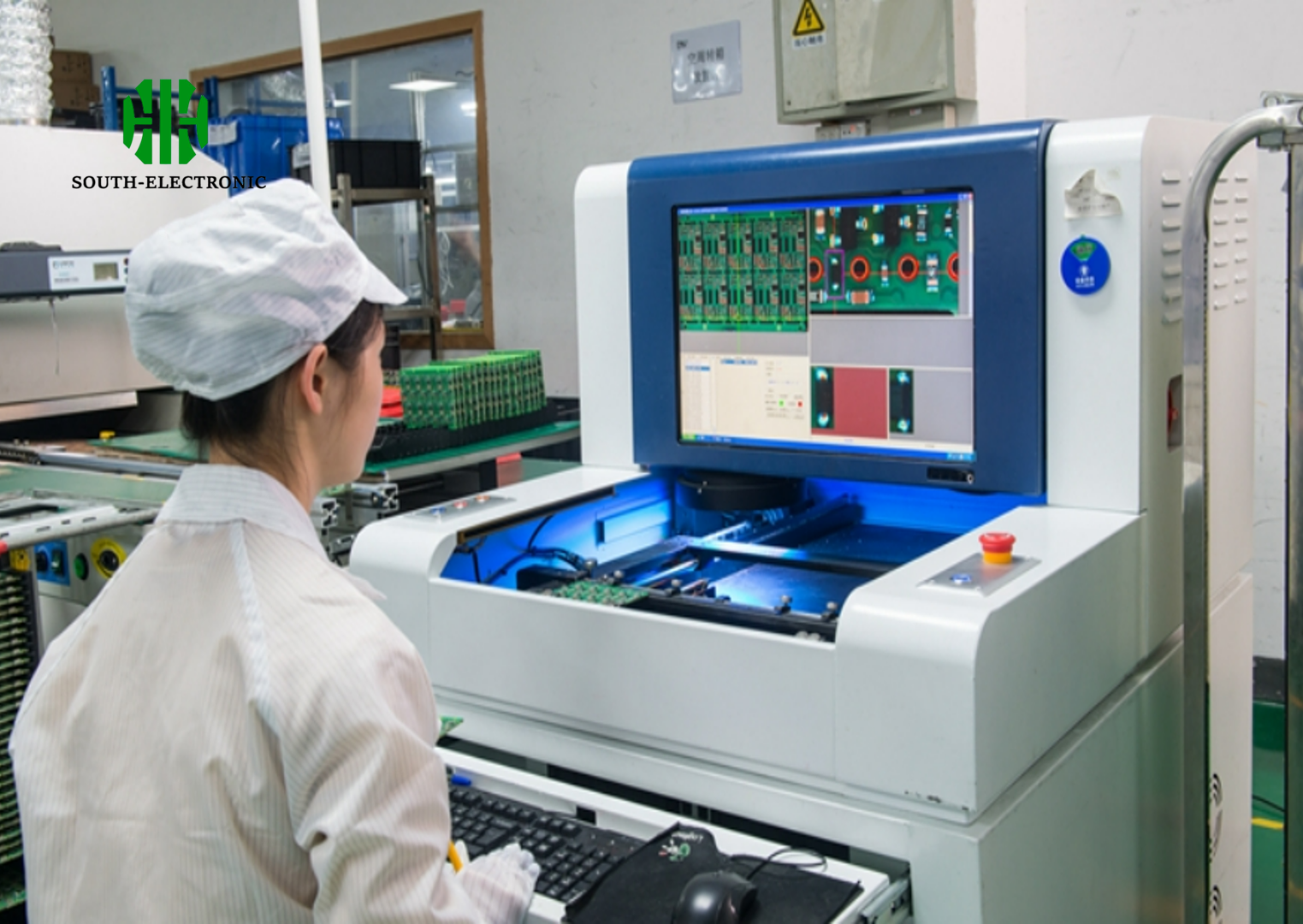
Visual Inspection: Initially, PCB is visually inspected to detect any obvious defects such as misalignments, smudges, or incorrect component placements. This is often done both manually by skilled technicians and using automated systems like Automated Optical Inspection (AOI).
Automated Optical Inspection (AOI): AOI machines use high-resolution cameras to inspect the surface of the PCB for defects such as scratches, thin solder, or missing components. This method is highly effective at catching issues early in the production process.
X-ray Inspection: This method is used primarily for inspecting multi-layer PCB and soldering quality under components like BGAs (Ball Grid Arrays). X-ray inspection helps identify issues like internal misalignment and hidden solder defects.
Electrical Testing: Electrical functionality is tested using bed-of-nails test fixtures or flying probe testers. These tests check for shorts, opens, resistance, capacitance, and other electrical parameters to ensure the PCB performs as designed.
In-Circuit Testing (ICT): ICT involves checking individual components on the board to ensure they are operational and correctly installed. This is a more thorough testing phase that can also program microcontrollers or other programmable devices on the PCB.
Functional Testing:After the PCB is assembled, it goes through functional testing. This is where the whole board is tested under normal operating conditions to make sure everything works the way it’s supposed to.
Environmental Stress Testing: This testing includes exposing the PCB to extreme temperatures, humidity levels, and vibrations to ensure stability and reliability under harsh conditions.
Burn-in Testing: Some PCB undergo burn-in testing, which involves running the board at high power and temperature for an extended period. This helps to identify early failures and ensure long-term reliability.
Ensuring Durability and Functionality in Consumer Electronics
To ensure that PCB used in consumer electronics are both durable and functional over their expected lifetimes, manufacturers implement several strategic measures:
Use of High-Quality Materials: Choosing the right base materials and components that can withstand environmental stress and wear over time is crucial.
Robust Design Practices: Employing advanced PCB design techniques such as proper trace routing, adequate spacing, and the use of thermal relief pads to mitigate issues of heat stress and physical damage.
Protective Coatings: Applying conformal coatings to protect against moisture, dust, and chemical contaminants, which can degrade the PCB over time.
Thorough Quality Assurance Protocols: Implementing comprehensive quality assurance processes at each stage of the manufacturing process, from initial design checks to final output testing, ensures that the PCB are free from defects and meet all performance criteria.
Feedback and Continuous Improvement: Regularly collecting feedback from testing phases and from the market allows manufacturers to continuously improve their processes and product quality.
Chapter 7
PCB Assembly Techniques
SMT (Surface Mount Technology)
Surface Mount Technology (SMT) is a method for producing electronic circuits in which the components are mounted directly onto the surface of PCB. It has become the most widely used technique in the assembly of modern electronic devices due to its efficiency and effectiveness.
Advantages of SMT:
- Higher Component Density: SMT allows for a larger number of components to be assembled on both sides of the PCB, which is ideal for high-density designs.
- Smaller Component Size: SMT components are generally smaller than their through-hole counterparts, allowing for more compact circuit designs.
- Faster Production Speed: SMT can be highly automated, making the assembly process faster and more efficient.
- Improved Performance at High Frequencies: SMT components have shorter leads and smaller solder joints, which can be beneficial for high-frequency applications.
- Reduced Cost: Although the initial setup cost for SMT can be high, the faster production rates and reduced material cost can result in a lower cost per unit in high-volume production.
Challenges of SMT:
- Complex Setup and Higher Initial Cost: Setting up for SMT requires more sophisticated equipment and a higher initial investment.
- Limited Repairability: SMT components can be difficult to replace or repair due to their small size and dense configuration.
- Thermal Sensitivity: Some SMT components are sensitive to heat, which can complicate the soldering process.
Through-Hole Technology (THT)
Through-Hole Technology (THT) involves inserting leads of components through holes drilled in the PCB and then soldering them in place. This technique has been largely supplanted by SMT for mass production but remains useful in specific applications.
Advantages of THT:
- Strong Mechanical Bonds: The leads of the components going through the PCB make THT joints stronger and more suitable for components that might endure physical stress.
- Ease of Soldering and Repair: Through-hole soldering is generally simpler to perform and repair, which can be advantageous for prototypes and low-volume production.
- Better Heat and Voltage Tolerance: Components that handle higher voltages and heat are often better suited to THT because the design allows for better heat dissipation.
Challenges of THT:
- Lower Component Density: THT uses more space on the PCB because the holes must be drilled and the leads inserted through the board.
- Slower Assembly Speed: THT generally requires manual placement and soldering of components, which can be slower and more labor-intensive than SMT.
- Increased PCB Size and Cost: Due to its lower component density and the need for drilling holes, THT can lead to larger PCB and higher costs, particularly for complex circuits.
Combining SMT and THT
In practice, many modern PCB use a combination of both SMT and THT. This hybrid approach allows you to optimize both the mechanical strength and electrical performance of the PCB by leveraging the strengths of each assembly technique. For example, components that need to withstand mechanical stress or high temperatures might use THT, while most other components use SMT to save space and cost. This approach gives you robust, high-performance PCB that work well for a wide range of consumer electronics applications.
Chapter 8
Innovations in PCB for Consumer Electronics
Overview of PCB in Consumer Electronics
Printed Circuit Board (PCB) is the backbone of modern consumer electronics. These components form the foundation upon which various electronic components are mounted to create complex circuits. In consumer electronics, PCB is used in virtually every device, from smartphones and tablets to televisions and microwaves. The design and quality of a PCB determine the functionality, reliability, and performance of the device.
The role of PCB in consumer electronics cannot be overstated. They provide the necessary electrical connections for transistors, resistors, capacitors, and other components, enabling the sophisticated operations that modern devices perform. With advancements in technology, the complexity of consumer electronics PCB has increased, incorporating multi-layer boards that support more components in a compact space. This evolution has allowed for the development of smarter, more energy-efficient, and feature-rich devices that continue to transform everyday life.
Importance of PCB in Modern Consumer Devices
PCB is critical for the performance and durability of consumer electronics. They are meticulously designed to withstand the demands of daily use and the specific conditions under which different devices operate. For instance, a PCB used in a wearable device like a smartwatch must be highly durable and flexible, capable of enduring physical stress and environmental factors such as moisture and temperature variations.
Moreover, the importance of PCB extends beyond just functionality. In the consumer electronics industry, where market competition is fierce, the innovation in PCB design directly contributes to the commercial success of products. Advanced PCB can lead to smaller, faster, and more powerful electronics, appealing to consumers seeking the latest technologies. Additionally, the efficiency of a PCB affects the overall energy consumption of the device, which is a critical factor in compliance with global energy standards and consumer preferences for sustainable products.
In conclusion, PCB is indispensable in the development and enhancement of consumer electronics. They not only ensure that devices operate as intended but also play a significant role in the ongoing innovation and marketability of consumer products. As technology continues to advance, the role of PCB in consumer electronics is expected to grow even more, driving new capabilities in connectivity, performance, and user experience.
Chapter 9
Challenges in Consumer Electronics PCB
Miniaturization
As consumer electronics continue to shrink in size while increasing in functionality, PCB designers face the significant challenge of miniaturization. This trend requires integrating more components into a smaller area without compromising the device’s performance or the durability of the PCB.
- High-Density Interconnect (HDI) Boards: These are increasingly used to support the miniaturization trend, as they allow for finer lines and spaces, smaller vias, and more compact component placement.
- Advanced Packaging Techniques: Techniques such as chip-scale packaging (CSP) and ball grid arrays (BGA) are essential for reducing the footprint of individual components on the PCB.
- Design Complexity: With miniaturization, the complexity of routing and layer management increases significantly. Designers must use sophisticated CAD tools and simulation software to ensure that signal integrity and functionality are maintained.
Heat Dissipation
As electronic devices become more powerful and compact, the amount of heat generated by components increases. Effective heat management is crucial to prevent overheating, which can reduce the lifespan of components and affect device reliability.
- Thermal Management Techniques: Incorporating thermal vias, heat sinks, and thermal pads into the PCB design helps conduct heat away from critical components. Materials with higher thermal conductivity, like copper, are often used to enhance heat dissipation.
- Component Selection and Placement: Designers must carefully select components that generate less heat and optimize their placement on the PCB to facilitate better air circulation and heat distribution.
- Multilayer Designs: Adding more layers to the PCB can help spread out heat-generating components, which assists in managing thermal loads more effectively.
Environmental Concerns
The environmental impact of PCB manufacturing and disposal is a growing concern. Consumers and regulatory bodies are increasingly demanding that electronics be both environmentally friendly and sustainable.
- Lead-Free and Halogen-Free Materials: Moving away from lead-based solders and halogenated flame retardants is crucial. Manufacturers are adopting materials that are safer for both the environment and human health.
- Recycling and Reusability: Designing PCB to be easily recyclable at the end of their life cycle is becoming more important. This involves selecting materials that can be efficiently separated and recycled.
- Energy-Efficient Manufacturing Processes: Reducing the energy consumption and waste generated during PCB manufacturing is a critical goal. This includes optimizing production lines and using renewable energy sources where possible.
Addressing these challenges requires ongoing innovation and adaptation in PCB design and manufacturing processes. As technology advances, so too must the strategies used to overcome these obstacles, ensuring that consumer electronics continue to evolve in a way that meets both consumer expectations and environmental standards.
Chapter 10
Future of PCB in Consumer Electronics
Predictions for Future Developments and Market Trends
The future of PCB in consumer electronics is likely to be driven by several key developments and market trends:
Continued Miniaturization: The trend towards smaller, more compact devices is expected to persist, pushing the limits of current PCB technology. Innovations in nano-technology and micro-electronics will further enable the production of ultra-thin, flexible PCB that can be integrated into innovative device forms like wearable technology and even implantable devices.
Integration of Advanced Materials: As the functionalities required from consumer electronics continue to grow, the integration of new materials such as graphene, conductive polymers, and advanced composites will play a critical role. These materials offer superior electrical, thermal, and mechanical properties that can enhance the performance and durability of PCB.
Smart PCB: With the rise of the Internet of Things (IoT) and smart devices, PCB themselves will become ‘smarter’. This involves embedding sensors directly into the PCB, enabling real-time data collection and feedback, and the ability to monitor and adjust their performance autonomously.
AI and Machine Learning Integration: AI and machine learning will increasingly be used not just in the design and manufacturing of PCB but embedded within the PCB themselves for enhanced performance optimization, predictive maintenance, and better user interaction.
5G and Beyond: As telecommunications standards advance to 5G and beyond, PCB will need to support higher frequencies and faster data rates. This will require innovations in PCB layout, material science, and signal integrity management.
The Role of Sustainability and Recyclability in PCB Design
Sustainability is becoming increasingly important in PCB design, influenced by environmental regulations and consumer demand for greener products:
Eco-friendly Materials: There is a growing shift towards using materials that are less harmful to the environment. This includes the use of lead-free solders, halogen-free flame retardants, and biodegradable substrates for PCB manufacturing.
Design for Recycling: PCB are being designed for easier disassembly and recycling at the end of their lifecycle. This involves using fewer types of materials and designing in a way that components can be easily separated without damaging them, facilitating more efficient recycling processes.
Energy-Efficient Manufacturing: Manufacturers are increasingly looking to reduce the energy consumption of their production processes. This includes optimizing existing manufacturing techniques and adopting new technologies such as additive manufacturing, which can reduce waste and energy use.
Lifecycle Assessment: More companies are conducting full lifecycle assessments of their products to understand and mitigate the environmental impact from manufacture to disposal. This holistic approach helps manufacturers identify areas where improvements can be made and showcases their commitment to sustainability.
In conclusion, the future of PCB in consumer electronics will be characterized by technological advancements that not only enhance performance but also address environmental concerns. Embracing these trends and innovations will be crucial for manufacturers seeking to remain competitive in a rapidly evolving market.
Start Your PCBA Project
The more detailed you fill out, the faster we can move to the next step.
