
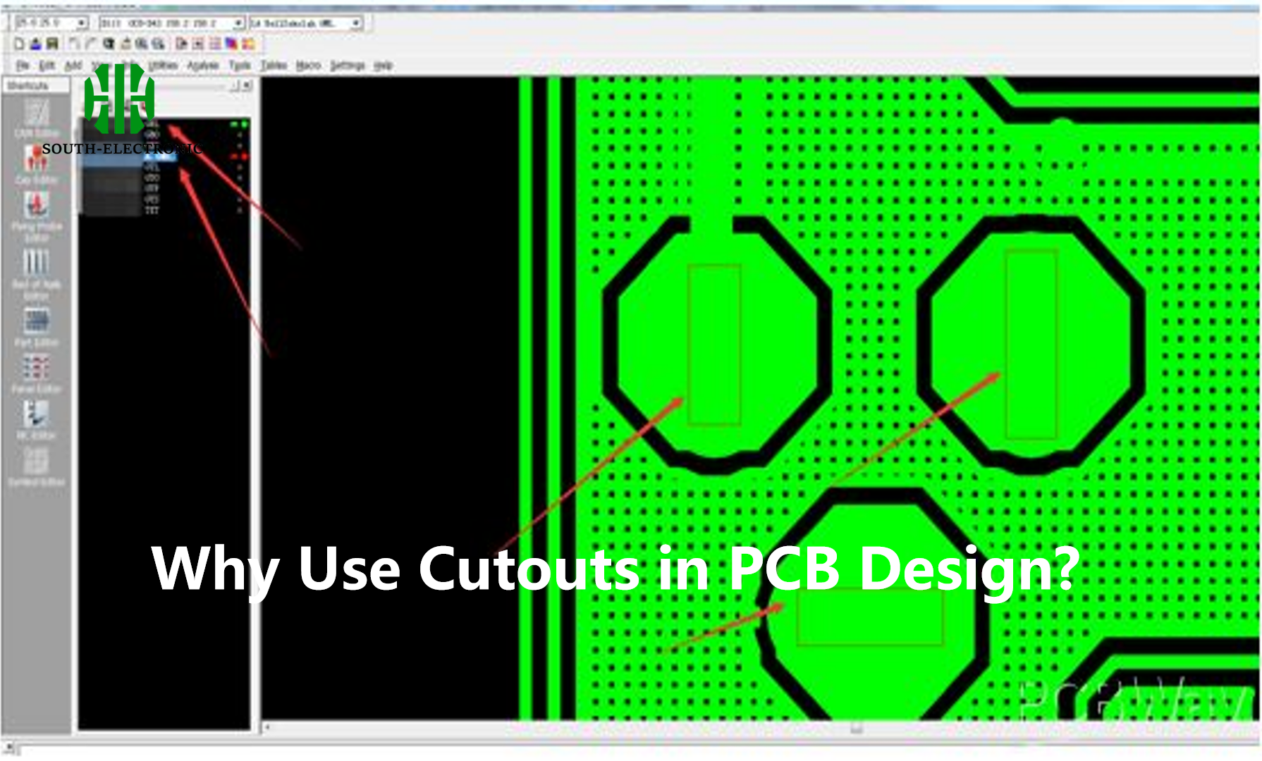
Why Use Cutouts in PCB Design?
Cutouts are an essential feature in PCB design, providing mechanical, electrical, and cost-related benefits. From weight reduction to improved thermal management, cutouts play a vital role in optimizing the performance and manufacturability of PCBs. By carefully considering the placement, size, and shape of cutouts, designers can achieve more efficient, reliable, and cost-effective designs. Whether used for cable routing, component clearance, or thermal management, cutouts are a versatile tool in the PCB designer’s arsenal.
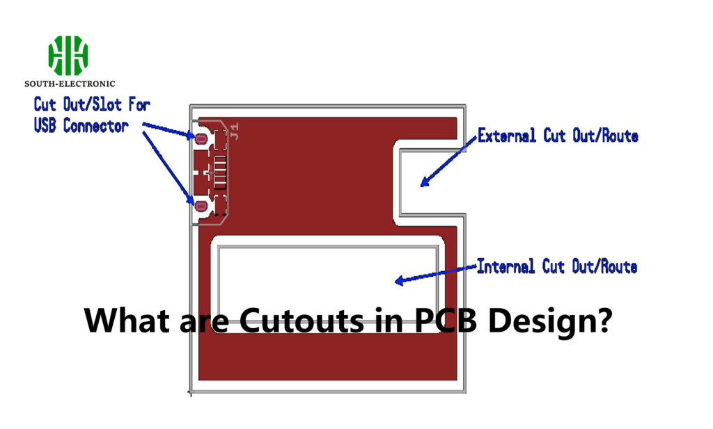
What are Cutouts in PCB Design?
When we talk about cutouts in PCB design, we’re referring to holes or voids that are intentionally created in the PCB material. These cutouts can come in all shapes and sizes, depending on the specific design requirements. Some common types of cutouts include rectangular, circular, and irregular shapes, each serving a unique purpose. For example, a rectangular cutout might be used to accommodate a connector, while a circular cutout could be designed to reduce weight or improve thermal dissipation.
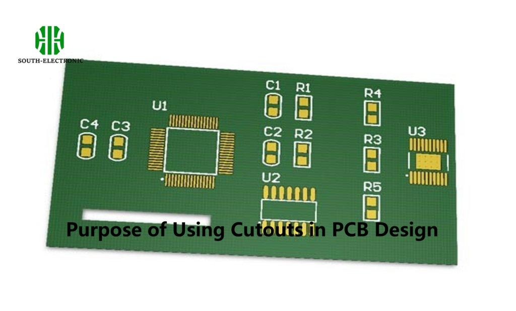
Purpose of Using Cutouts in PCB Design
Mechanical Considerations
- Weight Reduction: One of the primary mechanical reasons for incorporating cutouts in a PCB is to reduce its overall weight. In applications where weight is a critical factor, such as in aerospace or portable electronic devices, even small reductions in weight can be significant. By strategically removing material that does not contribute to the structural integrity of the PCB, designers can achieve weight savings without compromising the board’s functionality.
- Mounting Considerations: Cutouts are also essential for facilitating the mounting of components or assemblies onto the PCB. For instance, a cutout might be placed to allow a mechanical fastener to pass through the board or to accommodate the shape of a component that extends below the surface of the PCB. This ensures a secure fit and prevents any interference with other components on the board.
Electrical Considerations
- Isolation: Electrical isolation is another critical consideration in PCB design. Cutouts can provide this isolation by physically separating conductive areas, reducing the risk of short circuits or unintended electrical interference. This is particularly important in high-density PCBs where space is limited, and the risk of electrical crosstalk is higher.
- Heat Dissipation: Effective thermal management is crucial in PCB design, especially in high-power applications where components can generate significant heat. Cutouts can play a vital role in enhancing thermal dissipation by allowing heat to escape more efficiently from the PCB. This helps prevent overheating, ensuring that components operate within their optimal temperature range and improving the overall reliability of the device.
Cost Considerations
- Material Savings: By removing unnecessary material, cutouts contribute to cost savings during the PCB manufacturing process. Using less material not only reduces production costs but also results in a lighter, more efficient design, which can be particularly beneficial in large-scale production.
- Manufacturing Efficiency: Cutouts can also streamline the manufacturing process by simplifying the PCB design. For example, removing areas that are difficult to fabricate or assemble can make the production process faster and more efficient. This, in turn, reduces overall manufacturing costs and improves the consistency of the final product.
Impact of Cutouts on PCB Cost and Weight
| Design Aspect | With Cutouts | Without Cutouts | Percentage Change |
|---|---|---|---|
| Material Cost | $1000 | $1200 | -16.7% |
| PCB Weight (grams) | 250 | 300 | -16.7% |
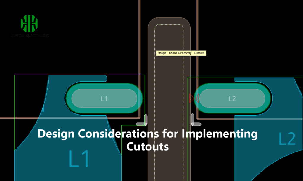
Design Considerations for Implementing Cutouts
Structural Integrity
When designing cutouts in a PCB, it is essential to ensure that the structural integrity of the board is not compromised. While cutouts can reduce weight and material usage, they can also weaken the PCB if not placed correctly. Designers must carefully evaluate the trade-offs between weight reduction and strength to avoid creating potential failure points in the PCB.
Manufacturing Constraints
Cutouts must be compatible with the chosen PCB manufacturing process. The minimum size and shape of cutouts may be limited by the capabilities of the fabrication equipment. Designers should work closely with manufacturers to ensure that the cutouts can be produced accurately and consistently, without causing delays or increasing production costs.
Placement Guidelines
The placement of cutouts should be strategic to avoid interference with components or electrical traces. For example, placing a cutout too close to a critical trace could introduce unwanted electrical noise or reduce the effectiveness of shielding. Designers should use simulation tools to analyze the effects of cutouts on the PCB’s performance and make adjustments as needed.
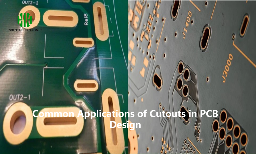
Common Applications of Cutouts in PCB Design
- Connector and Cable Routing:Cutouts are often used to facilitate the routing of connectors and cables through the PCB. This is particularly common in multi-layer PCBs, where space is limited, and routing paths are complex. By providing clear paths for cables and connectors, cutouts help to simplify the assembly process and reduce the risk of signal interference.
- Thermal Management:In power electronics, where components can generate significant heat, cutouts are used to enhance thermal management. For example, a cutout might be placed directly under a high-power component to allow heat to dissipate more efficiently. This helps to prevent overheating and ensures the reliability of the device.
- Component Clearance:Larger components, such as transformers or heat sinks, often require additional space on the PCB. Cutouts can be used to provide this clearance, allowing the components to fit without interfering with other parts of the PCB. This is particularly important in compact designs where space is at a premium.
- Antenna Clearance:In wireless devices, the performance of antennas can be significantly affected by the surrounding PCB material. Cutouts are often used to create clearance around antennas, reducing the impact of the PCB on the antenna’s performance and improving signal strength.
Comparison of Different Cutout Shapes and Their Applications
| Cutout Shape | Common Applications | Benefits |
|---|---|---|
| Rectangular | Connector routing, mounting holes | Easy to manufacture, versatile |
| Circular | Weight reduction, heat dissipation | Uniform stress distribution, simple |
| Irregular | Custom component clearance | Maximized space utilization |
When you design a PCB, you have to think about a lot of things. You have to think about how the board is going to be laid out physically, how all the electrical connections are going to be made, and how you’re going to manage the heat. One thing that is often overlooked but can make a big difference in how well your board performs is the use of cutouts.

