Ever struggled with achieving sufficient power amplification without distortion? Modern devices demand precision signal boosting. Multi-stage amplifiers solve this by combining gain stages – but poor design causes instability.
Designing multi-stage amplifiers[^1] requires strategic stage sequencing, impedance matching[^2], and bandwidth optimization. Cascaded Common Emitter + Common Collector stages often provide optimal voltage gain and output stability while managing frequency response limitations.
Mastering multi-stage designs requires addressing five critical challenges. Let’s break down each key aspect professionals often overlook in real-world implementations.
What Are the Key Design Considerations When Cascading Amplifier Stages?
Stage stacking seems simple until phase shifts accumulate. I once ruined a microphone preamp by ignoring interstage loading effects – the harsh distortion taught me vital lessons.
Critical considerations include stage topology selection (CE/CC/CB), impedance relationships, filtering needs, and distortion management[^3]. Cascode configurations excel at high-frequency designs by minimizing Miller capacitance effects.
)
Stage Configuration Trade-offs
Three primary factors determine stage combination effectiveness:
| Parameter | CE Stage | CC Stage | Cascode |
|---|---|---|---|
| Voltage Gain | High (50-200) | Low (<1) | Very High |
| Bandwidth | Moderate | Wide | Wide |
| Input Impedance | Medium | High | Medium |
| Best Used For | Initial Stages | Output Buffers | RF Applications |
CE-CC combinations balance gain and stability, while cascode designs (CE-CB) prevent high-frequency roll-off. Always calculate total phase shift – exceeding 180° causes oscillation at unity gain frequencies.
Practical Implementation Tips
- Insert high-pass filters between stages to block DC offsets
- Use emitter degeneration resistors for gain stability[^4]
- Simulate AC sweeps to identify resonance points
- Apply negative feedback[^5] judiciously to flatten frequency response
How to Calculate Total Gain & Bandwidth in Multi-Stage Configurations?
Gain multiplication looks great on paper until bandwidth crashes. My first 3-stage amp design promised 80dB gain but only worked below 10kHz – classic newbie error.
Total voltage gain = Product of individual stage gains. System bandwidth ≈ 1/√(1/BW₁² + 1/BW₂² + …). Dominant pole approximation often guides practical bandwidth estimates in multi-stage designs.
)
Gain-Bandwidth Optimization
Key formulas and relationships:
| Calculation | Formula | Example (3-Stage) |
|---|---|---|
| Total Voltage Gain (Av) | Av₁ × Av₂ × Av₃ | 50 × 30 × 10 = 15,000 |
| -3dB Bandwidth (BW_total) | 1/√(1/BW₁² + 1/BW₂² + 1/BW₃²) | 1/√(1/100k² + 1/50k² + 1/200k²) ≈ 38kHz |
Design Heuristics
- Allocate more bandwidth to later stages
- Use current buffers between high-gain stages
- Bootstrap capacitive loads to maintain bandwidth
- Parallel devices in output stages for current drive
Why Does Impedance Matching Between Stages Matter?
Mismatched impedance robbed 30% gain in my early headphone amp prototype. Voltage transfer suffers when stages "fight" each other's impedance.
Proper interstage matching maximizes power transfer and prevents loading effects. Rule: Next stage’s input impedance ≥ 10× previous stage’s output impedance for <10% gain loss.
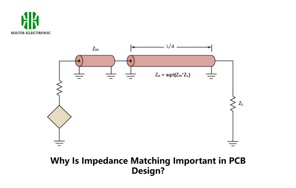
Matching Strategies
Effective techniques vary by frequency range:
| Frequency Range | Best Method | Typical Application |
|---|---|---|
| DC – 1MHz | Resistor Dividers | Audio Amplifiers |
| 1MHz – 100MHz | Transformer Coupling | RF Amplifiers |
| >100MHz | Transmission Lines | Microwave Circuits |
Practical Checks
- Measure input/output impedance with network analyzer
- Use Darlington pairs for high Z_in
- Implement selective negative feedback
- Add trimmer pots for laboratory prototypes
What Power Supply Considerations Are Critical for Multi-Stage Designs?
I learned about ground loops the hard way – a 120Hz hum ruined my first PA system. Proper power distribution[^6] prevents such nightmares.
Critical factors include: Supply decoupling, ground plane design, current headroom (20% minimum), and thermal management[^7]. Dual supplies enable direct-coupled stages without blocking capacitors.
)
Power System Checklist
| Stage Type | Decoupling Needs | Voltage Stability |
|---|---|---|
| Input Stages | 100nF ceramic + 10μF | ±1% regulation |
| Driver Stages | 10μF electrolytic | ±5% minimum |
| Output Stages | 1000μF + 0.1μF | High current capability |
Common Pitfalls
- Shared return paths causing oscillation
- Insufficient bulk capacitance during transients
- Voltage drops across PCB traces
- Thermal runaway in Class AB stages
How to Validate Amplifier Performance Using Practical Testing Methods?
Simulation lies. Bench testing revealed my "perfect" 1GHz bandwidth amp actually peaked at 650MHz due to layout parasitics.
Essential tests include: Frequency response sweeps, THD+N measurements, thermal imaging, and load step testing. Always validate under actual operating conditions.
)
Validation Protocol
| Test | Equipment Needed | Pass Criteria |
|---|---|---|
| DC Offset | DMM | 45° phase margin |
| THD at Full Power | Audio Analyzer | <0.1% @ 1kHz |
Debugging Tactics
- Probe intermediate nodes with high-Z active probes
- Use current mirrors to monitor stage consumption
- Apply input frequency sweeps while monitoring heating
- Check for oscillations with spectrum analyzer
Conclusion
Effective multi-stage amplifier design balances gain, bandwidth, and stability through careful stage selection, impedance management, and rigorous real-world testing. Prioritize system-level thinking over individual stage optimization.
[^1]: Explore how multi-stage amplifiers enhance audio quality and performance, ensuring distortion-free sound amplification.
[^2]: Understanding impedance matching can significantly improve your amplifier’s performance and efficiency, making it a crucial aspect of design.
[^3]: Learn about effective distortion management techniques to ensure high-quality audio output in your amplifier designs.
[^4]: Learning about emitter degeneration resistors can enhance your designs by ensuring consistent gain across stages.
[^5]: Understanding negative feedback is crucial for optimizing amplifier performance and achieving a flat frequency response.
[^6]: Understanding power distribution is crucial for preventing issues like ground loops and ensuring optimal performance in multi-stage amplifiers.
[^7]: Thermal management is vital for maintaining amplifier reliability and performance, especially in high-power applications. Explore this topic for better designs.