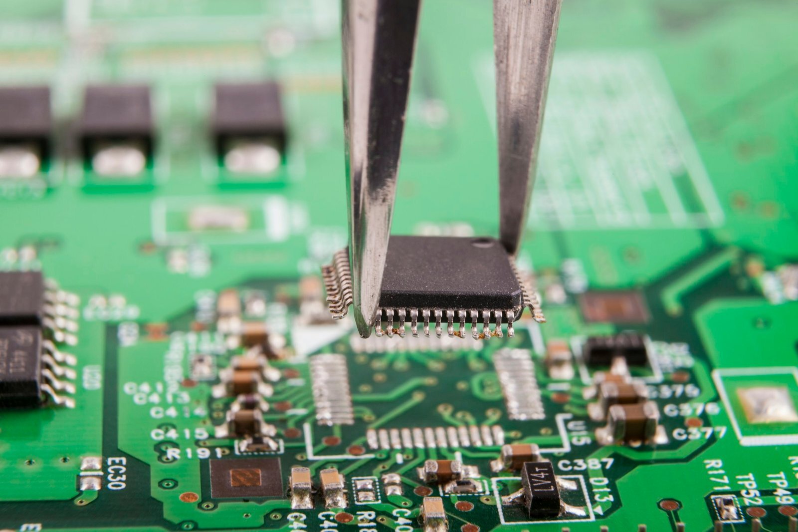
Missed DFM checks often lead to scrapped prototypes, delayed shipments, and blown budgets. After losing $4,200 on a capacitor spacing error, I learned hard lessons about pre-production verification.
Effective DFM checks[^1] require validating design rules, component placements, material selections, stackup symmetry, and assembly markers against your manufacturer’s equipment limits to eliminate fabrication errors and ensure cost-efficient PCB manufacturing[^2].
Let’s analyze the four critical DFM focus areas that separate successful prototypes from scrap piles.
Why Are Design Rules Critical to Avoid DFM Check Failures?
I once ignored a fab house’s 4mil trace width minimum, assuming all manufacturers could handle 3.5mil lines. The resulting open circuits taught me a harsh lesson.
Design rules[^3] define measurable constraints (trace widths, clearances, via sizes) ensuring your PCB matches factory capabilities. Violating these causes etching defects, short circuits, and impedance mismatches.

Key Design Rule Requirements
Break down critical DFM parameters into three categories:
| Category | Parameters | Typical Values |
|---|---|---|
| Conductors | Min trace width/space | 4-6mil (standard fab) |
| Vias | Drill size, annular ring | 8mil hole, 12mil pad |
| Clearance | Component-to-edge distance | 40mil (manual assembly) |
-
Trace Geometry
Avoid acute angles (4 layers – plating voids increase with depth. Use staggered vias for deep connections. -
Heat Dissipation[^7]
Balance copper pours in power layers. 70% fill in L3 and 30% in L4 creates uneven expansion rates during soldering.
Submit your stackup for pre-approval. One manufacturer modified our 6-layer design to use their standard 0.2mm prepregs, saving 3 weeks lead time.
Conclusion
Thorough DFM checks validate design rules, intelligent placement, material compatibility, and balanced stackups. Partner early with manufacturers to convert theoretical designs into manufacturable, cost-effective PCBs – your bottom line will thank you.
[^1]: Understanding DFM checks can significantly reduce errors and costs in PCB production, ensuring a smoother manufacturing process.
[^2]: Staying updated on PCB manufacturing trends can enhance your production efficiency and keep you competitive in the market.
[^3]: Exploring the importance of design rules can help you avoid costly mistakes and improve the reliability of your PCB designs.
[^4]: Understanding SMT machine no-go zones is crucial for avoiding costly manufacturing errors and ensuring efficient assembly processes.
[^5]: Explore the advantages of high Tg materials to enhance your PCB designs and prevent issues like pad cratering.
[^6]: Understanding impedance control is crucial for high-speed PCB designs; learn how to optimize your layouts for better performance.
[^7]: Discover strategies for effective heat dissipation to improve the reliability and performance of your PCBs.


