
Your smartphone crashes during a video call. Your smartwatch freezes mid-workout. Behind every digital device failure lies hidden design secrets – and answers written in copper pathways.
A Digital PCB[^1] processes binary signals (0s/1s) using microprocessors, memory chips, and logic ICs. These circuit boards prioritize signal speed and timing precision while battling electromagnetic interference (EMI), forming the backbone of modern AI systems, 5G networks, and IoT devices.
Let me show you why these unassuming green boards make your tech work – and fail. We’ll break down four critical aspects every engineer should master when working with digital PCBs.
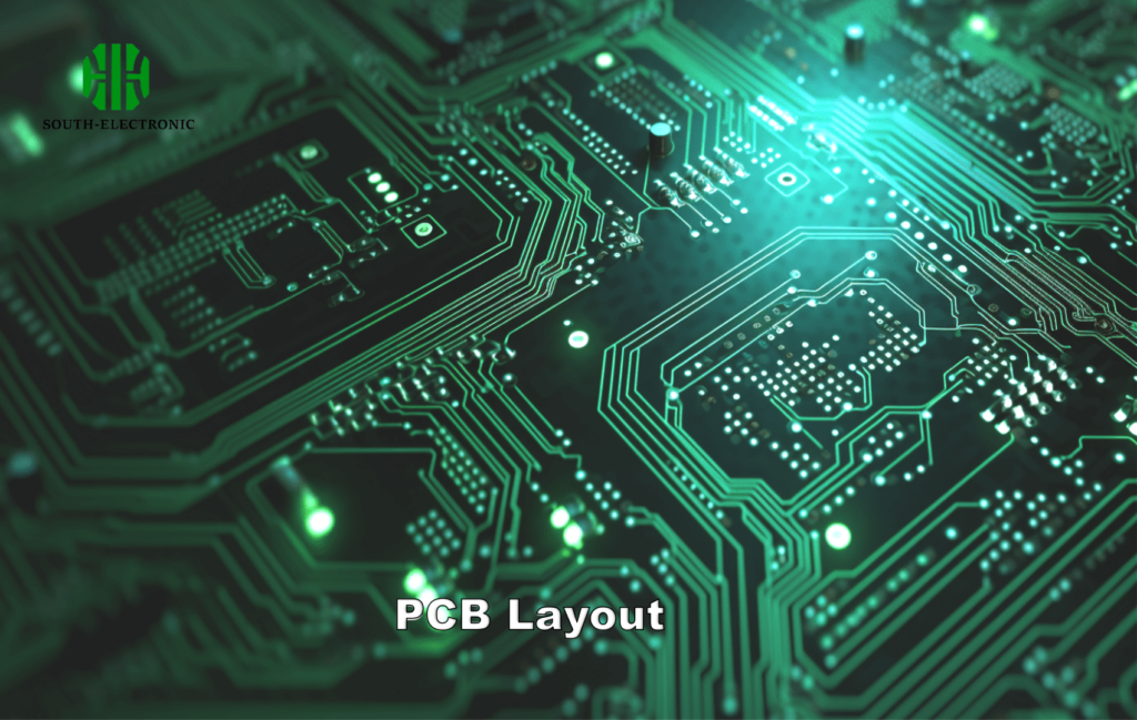
Why Do Digital PCBs Demand Unique Layout Rules?
Your new router keeps dropping signals despite perfect components. 85% of digital PCB failures trace back to layout errors – not parts quality.
Digital PCBs require precise trace routing and EMI shielding[^2] to prevent data corruption. Key rules include controlled impedance paths, strict length matching for clock signals, and strategic ground plane placement for noise reduction.
)
Digital PCB’s Three Layout Challenges
| Challenge | Consequences | Mitigation Strategies |
|---|---|---|
| EMI Radiation | Signal cross-talk | Shielding cans, guard traces |
| Heat Buildup | Processor throttling | Thermal vias, copper pours |
| Signal Skew | Timing errors | Length-matched serpentine traces |
High-speed signals act like radio antennas. I once designed a drone controller where Wi-Fi signals interfered with motor PWM signals. The fix? Separate analog and digital power planes with moats.
Clock signals need synchronized arrival times across components. A 1mm length mismatch in HD video processing caused visible screen artifacts. This equals 6 ps delay at 5 GHz signals.
Which Critical Components Power Digital PCBs?
Your gaming PC’s sudden reboot might not be software-related. Failed voltage regulators[^3] account for 40% of unexplained digital PCB malfunctions.
Essential digital PCB components include microcontrollers (MCUs)[^4], DDR memory modules[^5], oscillators for clock generation, and voltage regulators. Each requires specific handling during assembly to prevent signal integrity issues.
)
Core Component Specifications Table
| Component | Key Metric | Failure Impact |
|---|---|---|
| MCU | Clock speed | System freeze |
| Voltage Regulator | Ripple noise | Random resets |
| DDR RAM | CAS latency | Data corruption |
| Crystal Oscillator | Frequency stability | Communication drops |
Memory ICs need careful PCB pairing. During production testing, DRAM modules from different batches caused 15% failure rates due to timing variances. Always verify component revisions.
Power delivery remains critical. A server board prototype failed because its 3.3V regulator couldn’t handle sudden current spikes during CPU load shifts. The solution? Parallel MOSFET arrays.
How Do Digital PCBs Enable Modern Tech?
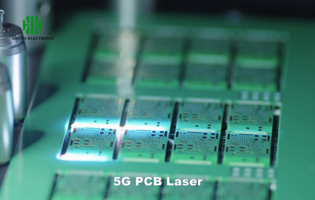
That 5G tower near your home handles 20,000 simultaneous connections. Its secret? Digital PCBs with 60-layer stacking managing terabit data flows.
Digital PCBs enable AI accelerators through parallel processing arrays. They support IoT networks via integrated RF modules. 5G systems rely on PCBs that manage mmWave signal paths shorter than 5mm with 0.2mm via spacings.
)
Technology Enablement Factors
| Technology | PCB Requirement | Example Application |
|---|---|---|
| AI/ML | High-speed interconnects | GPU cluster boards |
| IoT | Mixed-signal design[^6] | Smart sensors |
| 5G | Low-loss dielectric materials | Base station beamformers |
| Automotive | Flexible substrates | ADAS control units |
A neural network accelerator board required 128 parallel memory channels. Conventional layouts left 35% traces unmatched. The breakthrough came with 3D microvia stacking[^7].
Can Digital PCBs Work Alone?
Your wireless earbud case blinking red? Its digital PCB needs help from analog companion circuits for real-world operations.
Digital PCBs require analog support circuits[^8] for practical functionality. Power management, sensor interfaces, and RF modules are usually analog-based, working with digital cores through ADCs/DACs.
System Integration Partners
| Interface | Hardware | Bridge Component |
|---|---|---|
| Power | Battery/PSU | PMIC |
| Environment | Sensors | ADC |
| Wireless | Antenna | RF Front-End |
| Human | Touchscreen | Display driver IC |
A smart factory robot’s digital brain couldn’t adjust grip strength until we paired it with analog force sensors. The final design used 12-bit ADCs sampling at 1 kHz.
Conclusion
Digital PCBs power our tech-driven world through precise signal handling and speed optimization. Success requires smart layouts, quality components, analog partnerships – and engineers understanding these hidden battles.
[^1]: Understanding Digital PCBs is crucial for grasping modern electronics. Explore this link to deepen your knowledge on their design and functionality.
[^2]: EMI shielding is vital for preventing signal interference. Discover effective strategies to enhance your PCB designs by exploring this resource.
[^3]: Understanding voltage regulator issues can help prevent malfunctions in your digital PCB designs. Explore this resource for insights.
[^4]: Discover the importance of MCUs in digital PCB design and how they influence system performance and stability.
[^5]: Learn how DDR memory modules impact performance and reliability in digital PCBs, crucial for optimizing your designs.
[^6]: Understanding mixed-signal design is crucial for integrating analog and digital circuits effectively in PCBs.
[^7]: Explore how 3D microvia stacking can enhance PCB performance and solve layout challenges.
[^8]: Learn why analog circuits are essential for the functionality of digital PCBs in real-world applications.

