
Custom 2-Layer PCB Manufacturing Services
Min trace 3/3 mil | ENIG / HASL | FR-4 & High-TG | AOI & E-Test
We manufacture high-precision 2-layer PCBs suitable for a wide range of applications, including consumer electronics, automotive, and industrial devices. Our commitment to stable quality and consistent performance ensures reliable production runs tailored to your needs.
2-Layer PCB Capabilities
2-Layer PCB Process Capability
-
Layer Count
2 layers
-
PCB Dimensions
≤24*48inch(610*1220mm)
-
Materials Types
FR-4 | High Tg | Halogen-free | Flexible PCB | Aluminum substrate material
-
Material Brand
Lianmao | Shengyi | Taiyao | Nanya, Panasonic | Isola | Nelco | Rogers | Taconic | Arlon...
-
Board Thickness
0.2 mm - 8.0 mm
-
Finish Treatment
Immersion Gold | Lead-free HASL | OSP | Immersion Tin | Immersion Silver | Thick Gold Plating | Silver Plating | Immersion Gold + OSP
-
Copper thickness
0.5 OZ - 6 OZ
-
SolderMask Color
Green | Blue | Black | Yellow | Red | Purple | White...
-
Finish Treatment
Immersion Gold | Lead-free HASL | OSP | Immersion Tin | Immersion Silver | Thick Gold Plating | Silver Plating | Immersion Gold + OSP
Why Choose Us for 2-Layer PCB Manufacturing
We support engineers with reliable 2-layer PCB manufacturing,
from prototype builds to stable repeat production.
Every 2-layer PCB undergoes a thorough review by our engineering team to ensure stack-up integrity, impedance control, and manufacturability prior to production.
We emphasize consistent quality across all batches, enabling us to effectively support both prototype development and long-term production runs.
Our expertise includes managing tight trace/space requirements, controlled impedance, and multilayer lamination, ensuring complex designs are executed flawlessly.
We provide transparent technical communication and fast responses to effectively support overseas engineering and purchasing teams.
Related Project We Had Done
2-Layer PCB for Industrial Control System
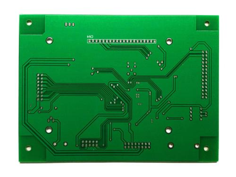
Application
Key Specs
Challenge
Result
2-Layer PCB for Consumer Electronics
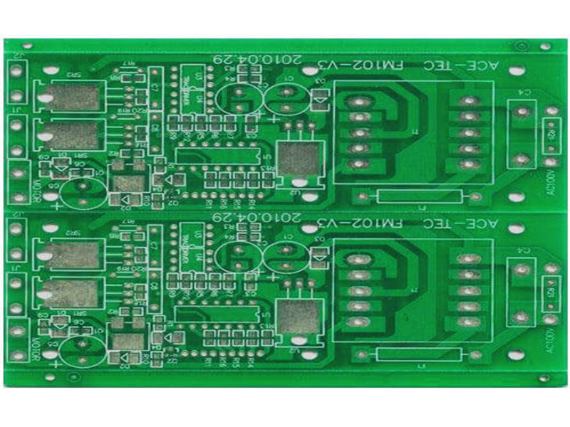
Application
Key Specs
Challenge
Result
2-Layer PCB for IoT Device
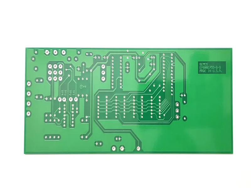
Application
IoT Gateway & Communication Device
Key Specs
Challenge
Result
Quality Control & Certifications for 2-Layer PCB Production
Common Questions
Most Popular Questions
What is the typical lead time for 2-layer PCB production?
What applications are suitable for 2-layer PCBs?
What material options are available for 2-layer PCBs?
How is quality control conducted for 2-layer PCBs?
Can I customize 2-layer PCBs?
Send Us a Message
The more detailed you fill out, the faster we can move to the next step.
