
Can outdated PCB curricula leave engineers unprepared for smart factories? Factories now demand adaptive designers fluent in AI and green practices. The skills gap is widening—fast.
By 2025, PCB education must prioritize design-for-manufacturability (DFM)[^1], AI-aided optimization tools[^2], and flexible circuit development while embedding lifecycle sustainability[^3]. Industry-aligned micro-certifications will bridge smart hardware and green manufacturing skill gaps.
)
But how do we transform traditional PCB training into next-gen skill factories? Let’s dissect three critical pillars reshaping engineering education.
PCB Education Development Process: Are Current Systems Future-Ready?
Most PCB programs still teach 2010-era workflows. Imagine students learning manual routing while factories deploy AI-driven DFM checks. Urgent modernization is overdue.
Future PCB education must integrate iterative prototyping with simulation tools, emphasize cross-domain collaboration (mechanical/thermal), and adopt agile certification frameworks to align with Industry 4.0 manufacturing realities.
Three Critical Gaps in Current PCB Training
| Skill Gap | Industry Need | Educational Solution |
|---|---|---|
| DFM Awareness[^4] | 73% of designs fail factory tests | Embedded CAM tool simulations |
| Multiphysics Analysis | Thermal/EMI issues delay 40% of projects | Unified PCB-CAD-FEA platforms |
| Agile Certification | 6-month tech refresh cycles | Modular micro-credentials (IPC/AI) |
Traditional programs focus on schematic capture but neglect manufacturability. For example, designing a 12-layer HDI board requires simultaneous DFM rule checks—a skill absent in most syllabi. The solution? Partner with EMS providers to build virtual factory labs where students optimize designs against real-world yield metrics.
What IoT Skills Should PCB Education Focus on by 2025?
A smart thermostat PCB isn’t just circuits—it’s sensors, wireless stacks, and edge AI. Yet most courses treat IoT as an "extra module."
PCB engineers need IoT fluency[^5]: ultra-low-power design, RF layout for protocols like Matter/Thread, and lifecycle analysis for sustainable sensor networks.
%[IoT PCB with wireless modules](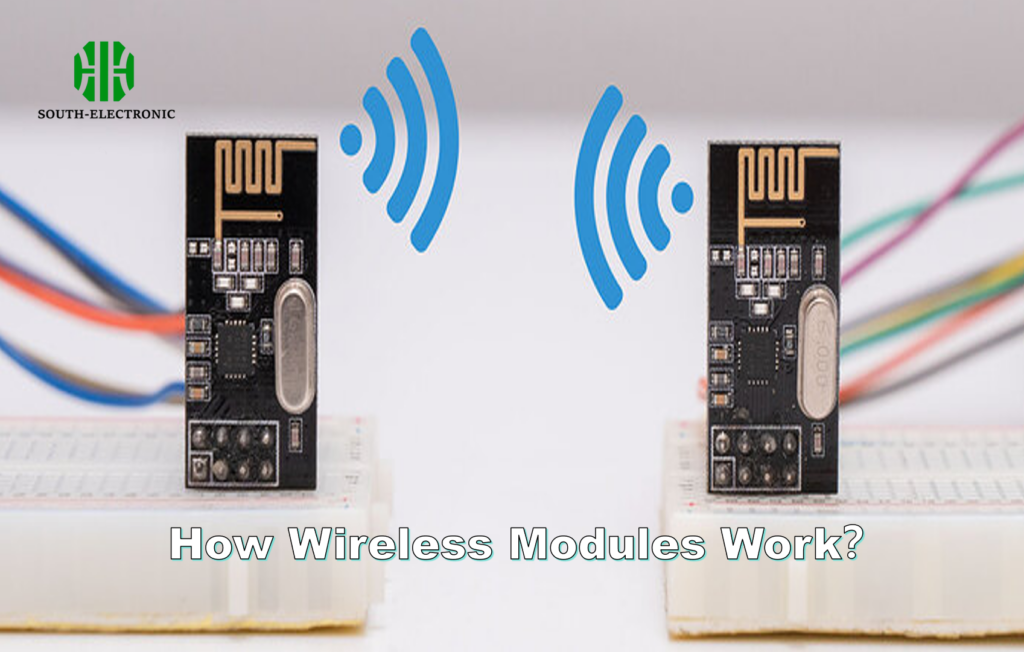 )
)
Building IoT-Ready PCB Skills
| IoT Skill | Educational Approach | Industry Impact |
|---|---|---|
| Energy Harvesting[^6] | Solar/BLE co-design projects | 60% longer sensor battery life |
| Embedded Security | Hardware-based encryption labs | Prevent 80% of firmware hacks |
| Eco-Materials | Biodegradable substrate experiments | Reduce e-waste by 35% |
IoT PCBs demand systems thinking. Take energy-aware design: students must balance MCU sleep modes, antenna efficiency, and thermal budgets. A Northeastern University pilot course reduced IoT power consumption by 41% using these methods.
Can AI Tutors Fix the PCB Educator Shortage Crisis?
Colleges struggle to hire PCB experts—the best work at NVIDIA or SpaceX. Result? 60% of schools reuse decade-old lectures.
AI tutors[^1] with domain-specific LLMs (trained on Altium/Mentor docs) can deliver personalized PCB training[^2], simulate expert mentorship, and update content hourly—scaling quality education globally.
)
AI Tutoring vs Traditional Models
| Aspect | Traditional Teaching | AI Tutor Advantage |
|---|---|---|
| Content Freshness | Updated every 2-3 years | Real-time IPC standard integration |
| Feedback Speed | Weeks for assignment reviews | Instant DFM violation alerts |
| Accessibility | Limited to class hours | 24/7 multilingual support |
An AI tutor named "PCB-GPT" developed by Siemens now assists 12 universities. It reduced student query resolution time from 48 hours to 9 minutes while cutting professors’ workload by 30%.
Conclusion
PCB education[^3] must merge AI-driven DFM tools, IoT systems thinking, and sustainable design into modular certifications—or risk graduating engineers for obsolete factories.
[^1]: Understanding DFM is crucial for engineers to create efficient designs that meet modern manufacturing needs. Explore this link to enhance your knowledge.
[^2]: AI tools are revolutionizing PCB design, making it essential for engineers to stay updated. Discover how these tools can enhance your skills.
[^3]: Lifecycle sustainability is key to modern manufacturing practices. Learn more about its importance and implementation in PCB education.
[^4]: Understanding DFM Awareness is crucial for improving PCB manufacturability and reducing design failures. Explore this link for in-depth insights.
[^5]: Gaining IoT fluency is essential for modern PCB engineers to design effective smart devices. Discover resources to enhance your skills.
[^6]: Energy Harvesting is key for sustainable PCB design. Learn about innovative practices that can extend battery life and improve efficiency.
[^7]: Explore how AI tutors can revolutionize PCB education by providing personalized learning experiences and real-time feedback.
[^8]: Learn about the advantages of personalized PCB training and how it can lead to better student outcomes and industry readiness.
[^9]: Discover the latest trends and innovations in PCB education that can enhance learning and prepare students for the industry.

