
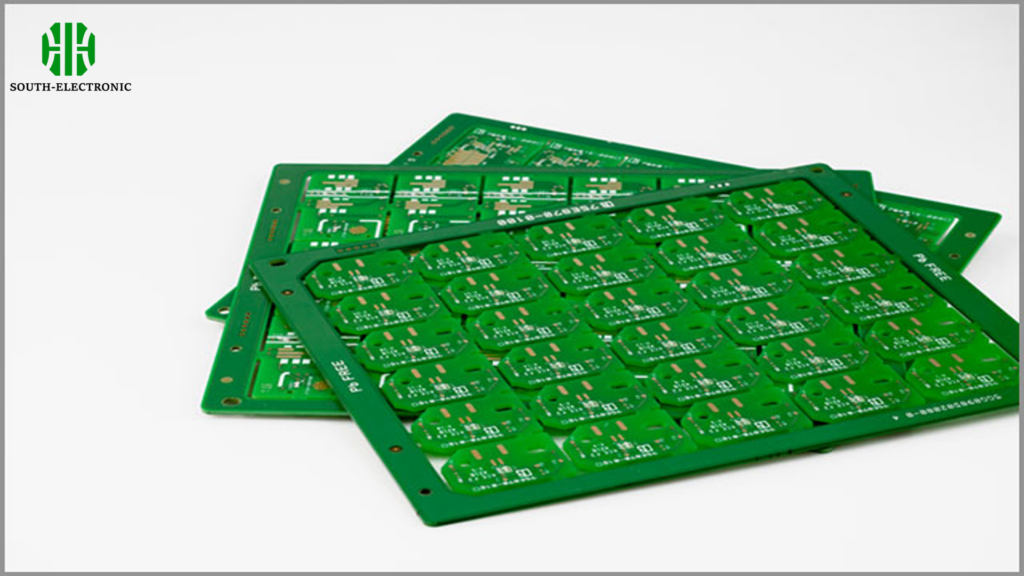
What is an Efficient PCB Manufacturing Process?
An efficient PCB manufacturing process involves precise and streamlined steps to design, print, and assemble printed circuit boards with minimal waste and maximum quality. This process typically includes designing the PCB with specialized software, layering and etching copper on a substrate, inspecting alignment and integrity, applying solder mask and silkscreen for protection and information, and conducting thorough testing for functionality and reliability before the final packaging and delivery. Each step is carefully controlled to ensure accuracy and adherence to technical specifications.
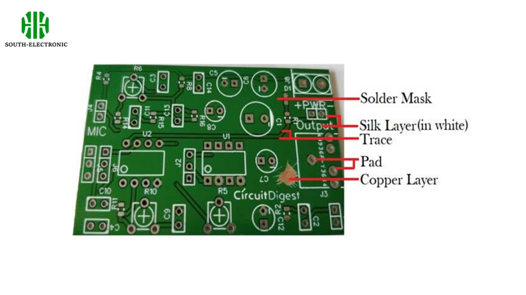
What are the Parts of a PCB?
A PCB consists of four primary components:
- Substrate: The foundational layer, typically made of fiberglass, which provides structural integrity and resistance to breaking.
- Copper Layer: This layer varies between copper foil and a full copper coating, depending on the PCB type, and functions similarly to the nervous system by transmitting electrical signals.
- Solder Mask: A protective polymer layer that safeguards the copper from short circuits by environmental contact.
- Silkscreen: Applied on the component side, this layer displays important information such as part numbers, logos, and testing points.
What is the Efficientt PCB Manufacturing Process?
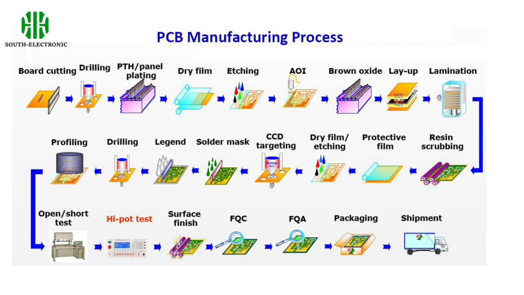
1.Board Cutting
- Description: Cutting the base material to the required size.
- Manufacturing Considerations: Ensuring dimensions are precise to avoid fit issues in final assembly.
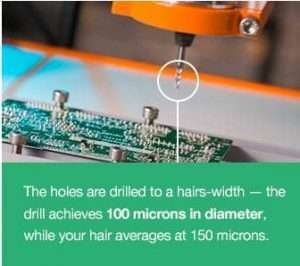
2.Drilling
- Description: Creating holes for mounting components and vias.
- Manufacturing Considerations: Accuracy in hole placement and size is critical for component alignment.
3.PTH/Panel Plating
- Description: Plating through-holes and vias to establish connectivity between layers.
- Manufacturing Considerations: Uniform plating is essential to ensure reliable electrical connections.
4.Dry Film
- Description: Applying a photo-sensitive film to layout the circuit patterns.
- Manufacturing Considerations: Film must adhere well and be evenly applied to avoid defects in patterning.
5.Etching
- Description: Removing unwanted copper to form the actual circuitry.
- Manufacturing Considerations: Controlling the etching process to maintain integrity of the circuit lines.
6.AOI (Automated Optical Inspection)
- Description: Checking for any missing traces, shorts, or other defects.
- Manufacturing Considerations: High accuracy in detection to ensure no defects are passed forward.
7.Brown Oxide
- Description: Treatment of the copper surface to improve adhesion before layering.
- Manufacturing Considerations: Ensuring even application to enhance lamination bond strength.
8.Lay-up
- Description: Assembling the different layers of the PCB.
- Manufacturing Considerations: Precise alignment of layers is crucial for functionality.
9.Lamination
- Description: Fusing the layers together under heat and pressure.
- Manufacturing Considerations: Optimal temperature and pressure settings to prevent delamination.
10.Resin Scrubbing
- Description: Cleaning the resin residue after drilling.
- Manufacturing Considerations: Complete removal of residues to avoid electrical issues.
11.Protective Film
- Description: Applying a protective layer to safeguard the circuitry during further processing.
- Manufacturing Considerations: Film must protect without leaving residues or affecting future processes.
12.Dry Film/Etching
- Description: Repeating the dry film and etching process for additional layers.
- Manufacturing Considerations: Consistency in application and etching across all layers.
13.CCD Targeting
- Description: Aligning layers using a camera coordination detection system.
- Manufacturing Considerations: Precision in alignment to avoid misregistration.
14.Solder Mask
- Description: Applying a solder mask over the copper traces.
- Manufacturing Considerations: Even application for protection and to prevent solder bridging.
15.Legend
- Description: Printing component identifiers and other markings.
- Manufacturing Considerations: Clarity and permanence of the text for ease of assembly and maintenance.
16.Drilling
- Description: Additional drilling for mounting holes or adjustment.
- Manufacturing Considerations: Precision to ensure no damage to the circuitry.
17.Profiling
- Description: Shaping the PCB to final dimensions.
- Manufacturing Considerations: Accurate cutting to match design specifications.
18.Open/Short Test
- Description: Testing for open circuits or shorts.
- Manufacturing Considerations: Comprehensive testing to ensure functionality.
19.Hi-pot Test
- Description: Applying high voltage to ensure insulation is effective.
- Manufacturing Considerations: Safety and precision in testing to detect potential failures.
20.Surface Finish
- Description: Applying a surface coating to protect against oxidation and to enhance solderability.
- Manufacturing Considerations: Choice of finish affects the durability and conductivity.
21.FQC (Final Quality Control)
- Description: Final inspection for defects.
- Manufacturing Considerations: Thorough inspection processes to meet quality standards.
22.FQA (Final Quality Assurance)
- Description: Assurance that all specifications are met.
- Manufacturing Considerations: Implementing strict quality protocols to ensure product reliability.
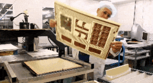
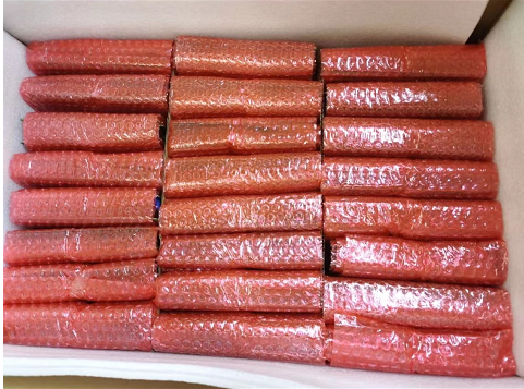
23.Packaging
- Description: Securing the PCBs for shipment.
- Manufacturing Considerations: Protective packaging to prevent damage during transport.
24.Shipment
- Description: Distributing the finished PCBs to clients or next-stage manufacturers.
- Manufacturing Considerations: Efficient logistics planning to ensure timely delivery.
Advancements in technology continue to drive innovations in Efficient PCB Manufacturing, meeting the growing demands for more complex and reliable electronic devices. The future of PCB manufacturing lies in the refinement of these processes and the integration of new materials and technologies

