

Ever had a device suddenly die? PCB failure feels like losing vital gear. My workshop faces this daily. But panic wastes time – my method salvages boards systematically.
I repair PCBs in five steps: inspect damage, clean affected areas, remove broken parts, fix circuitry, and test results. This logical approach restores functionality while preventing further harm.
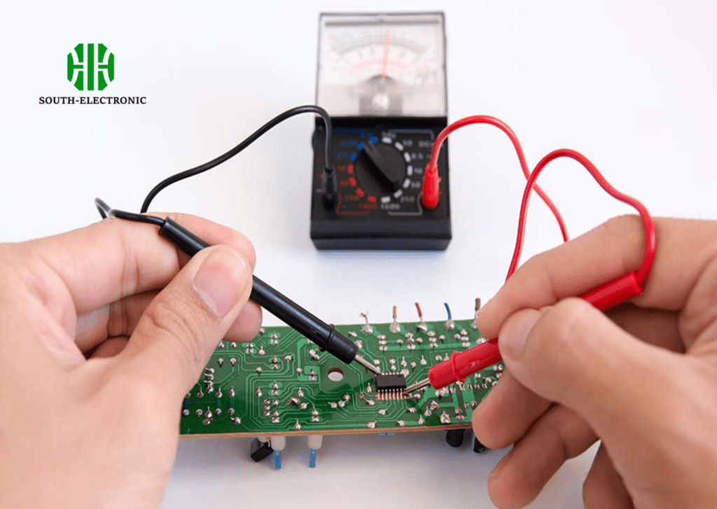
Don’t let complex repairs overwhelm you. I’ll explain these steps practically. Then we’ll cover specific challenges I often encounter.
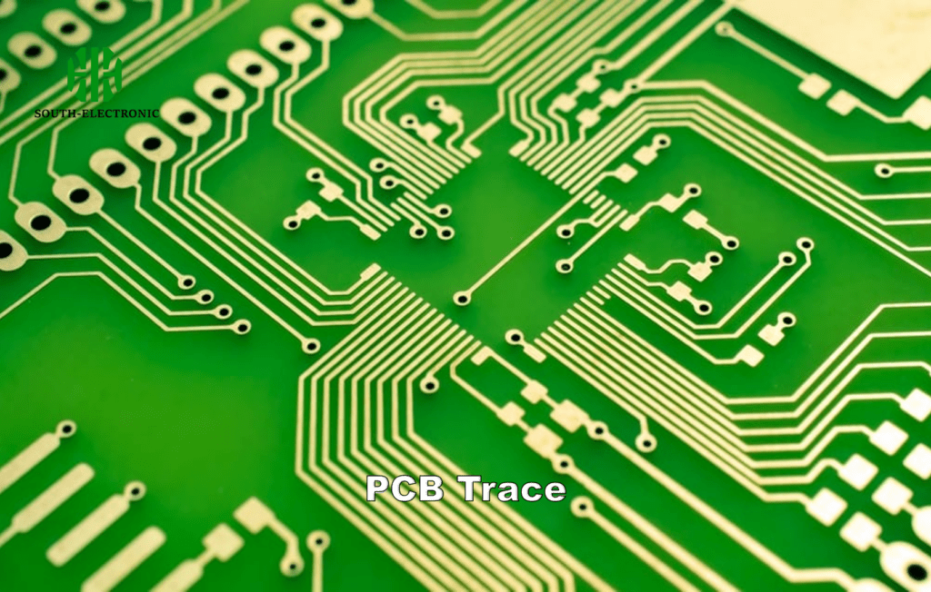
Can Burned or Damaged PCB Traces Be Repaired?
Burn marks on circuits look terminal. You worry replacement is the only option. I felt that dread early in my career.
Burned traces are fixable! I use jumper wires or conductive ink to rebuild paths. Essential tools: microscope, scalpel, and copper tape. Successful repairs restore full conductivity.
Most trace failures involve three components:
Repair Method Comparison
| Damage Type | My Approach | Tools Required |
|---|---|---|
| Single-layer break | Jumper wire | Enamel wire, soldering iron |
| Burnt section | Scrape/solder bridge | Fiberglass pen, flux |
| Tiny trace crack | Conductive paint | Microbrush, UV curing lamp |
Copper traces carry electricity. Burns interrupt this flow. My first drone controller had this issue. I locate unaffected connection points using a multimeter continuity test. Next I prepare the area by removing carbon residue with a fiberglass pen. For gaps under 2mm, I create solder bridges. Larger breaks need jumper wires attached to exposed pads. Always verify repairs under magnification for errors.
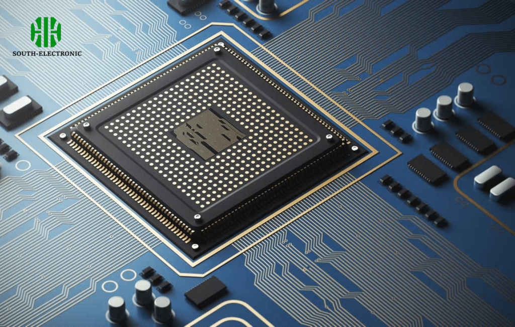
How to Repair Multilayer PCBs?
Multilayer boards intimidate many techs. Hidden inner layers seem unrepairable. I once thought so too – until learning these methods.
I repair inner layers by drilling access holes. Special epoxy anchors replacement vias. Critical: isolating damaged sections first. Pressure-sensitive films help locate breaks.
Layered PCBs require sequential analysis:
Layer Repair Techniques
| Layer Position | Access Method | Connection Solution |
|---|---|---|
| Surface layer | Direct soldering | Copper foil patches |
| Mid-layer | Micro-drilling | Plated through-hole vias |
| Power planes | Layer-edge probing | External bypass wires |
Each layer serves distinct functions. My GPS module failure taught me this. Start with schematic analysis to identify essential circuitry. Non-critical breaks remain unrepaired when possible. For vital inner traces, carefully drill 0.3mm test holes near suspected breaks. Injection needles apply conductive epoxy into voids. Post-repair impedance testing is crucial. I use network analyzers for RF boards. Thermal imaging checks for overheating in power layers.
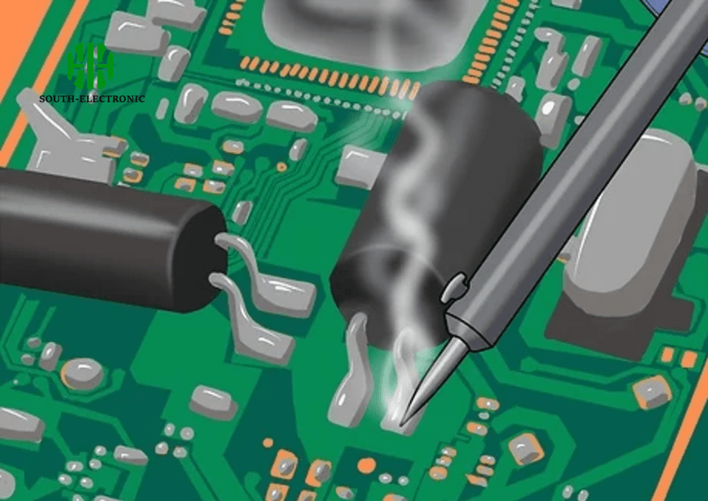
Why Do Solder Joints Fail?
Nothing frustrates like intermittent faults. Devices work then suddenly fail. Solder joints cause 70% of such issues in my experience.
Joints fail from mechanical stress, contamination, or thermal cycling. Poor craftsmanship accelerates this. Reflowing solves most cases but requires precise temperature control.
Solder problems manifest in predictable patterns:
Failure Causes & Fixes
| Failure Cause | Visual Signs | Repair Approach |
|---|---|---|
| Thermal fatigue | Cracked surface | Full joint resoldering |
| Contamination | Dull/grainy appearance | Cleaning and reflow |
| Mechanical stress | Lifted pads | Epoxy reinforcement |
| Cold solder | Irregular shape | Flux application and heat |
Solder forms metallic bonds between components. My first amplifier repair had cold joints. Vibration cracks these connections over time. Heat causes expansion mismatches between materials. Lead-free solder worsens this. I inspect joints under angled lighting. Contaminated joints appear porous. I clean them with isopropyl alcohol before reapplying solder. Thick boards require preheating to prevent pad lifting. Through-hole joints need fillet inspection – incomplete coverage risks failure.
Conclusion
My five-step PCB repair method works reliably: inspect, clean, remove, fix, test. Addressing trace damage, layer issues, and solder failures saves costly replacements. Practice makes perfect.


