Introduction
In recent years, the copper-clad laminate (CCL) industry has seen some pretty big changes. It's like the industry took a course in "How to Save the Planet 101," shifting towards eco-friendlier materials faster than a teenager updates social media. Enter 5G technology, strutting onto the scene to speed things up even more and promising to sprinkle a bit more innovation into the mix.
Importance
Electronic products have cozied up into every nook and cranny of our lives, and with the whole world chanting "Go Green!" the electronics sector has had to step up its game.
This movement gained momentum following the European Union's implementation of the RoHS and WEEE directives in July 2006. There's this global rulebook now, limiting the use of six villainous substances including lead and some brominated villains, pushing manufacturers towards greener pastures.The development of lead-free and halogen-free CCLs has been significantly accelerated, aligning with these new environmental standards.
Transitioning to lead-free processes poses challenges in maintaining the thermal resistance and reliability of CCLs, as they now need to endure the elevated temperatures associated with lead-free solder pastes. Switching to halogen-free materials has opened up a whole new adventure in chemistry, hunting for new flame retardants and tweaking resin recipes to keep CCLs in top form.

Revolutionizing the CCL Industry
The exponential advancement in chip technology, following Moore’s Law, has dramatically increased circuit integration over the last five decades. This evolution has nudged gadgets like smartphones and wearable tech to not just slim down for the digital runway but also smarten up, boasting precision and a bag of tricks t. It's an exciting time in the world of electronics, where the quest for compact, high-functioning devices meets the imperative of environmental stewardship. Who knew that going green could be so tech-savvy and stylish?
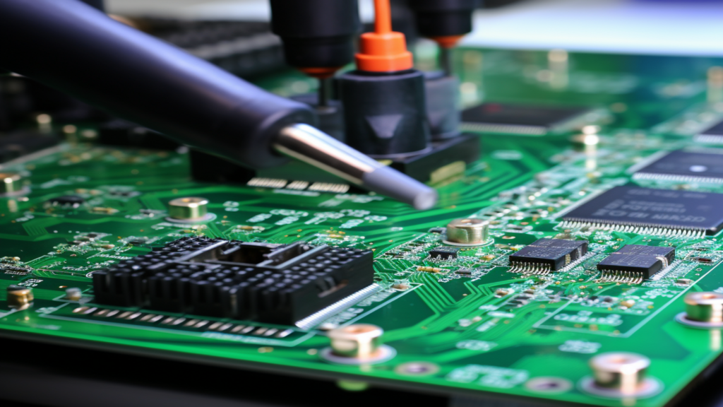
Consequently, printed circuit boards (PCBs), the foundational platforms for electronic circuits, must support high-density interconnections. This requirement has fueled the demand for CCLs that are not just thinner and lighter but also capable of handling the complexities of multi-layer or HDI PCBs.
Perfecting the slim profile of copper-clad laminates (CCLs) demands stringent oversight of the production line, from the exact application of adhesives to ensuring the materials are absolutely pure and that the base material remains perfectly flat and dimensionally consistent. To offset the limitations imposed by reduced size while enhancing performance, manufacturers often employ filler technologies or adjust resin formulations, customizing the performance of CCLs for specific applications.
In the rapidly evolving mobile communication sector, the expansion of the global user base has significantly driven the advancement of communication systems and materials. With each technological leap, roughly every decade, mobile communication technology advances, bringing about substantial improvements in data transmission rates and frequencies. In the era of 5G, we observe a shift to frequencies well beyond 5GHz or 20GHz, with data rates reaching 10-20Gbps or higher.
This evolution demands CCLs with superior electrical performance to meet the requirements of high frequency and speed. While standard CCLs suffice for applications operating below 1GHz, high-frequency, high-speed applications struggle with signal attenuation and require CCLs with specific electrical properties to prevent signal distortion or loss. Hence, the electrical performance of CCLs, especially in terms of low dielectric constants (Dk) and low dielectric loss factors (Df), is critical. The sector categorizes CCLs by their Dissipation Factor (Df) values, signifying the depth of material engineering required to satisfy the high standards set for data transmission at great speeds. This system of classification illuminates the nuanced understanding of material characteristics essential for developing cutting-edge electronic components.
Conclusion
Over the past decade, the journey of the CCL industry reflects a vibrant field quick to adapt to both technological progress and stringent environmental standards. Embracing eco-friendly, lead-free, and halogen-free materials, while also meeting the demands for high-frequency and swift applications in the age of 5G, showcases the industry's commitment to keeping pace with worldwide trends and the evolving technological landscape. As this sector moves forward, the ongoing advancement in CCL technology will be crucial in sculpting the future of the electronics industry, leading to the creation of electronic products that are both more environmentally sustainable and technologically advanced.

