
Introduction
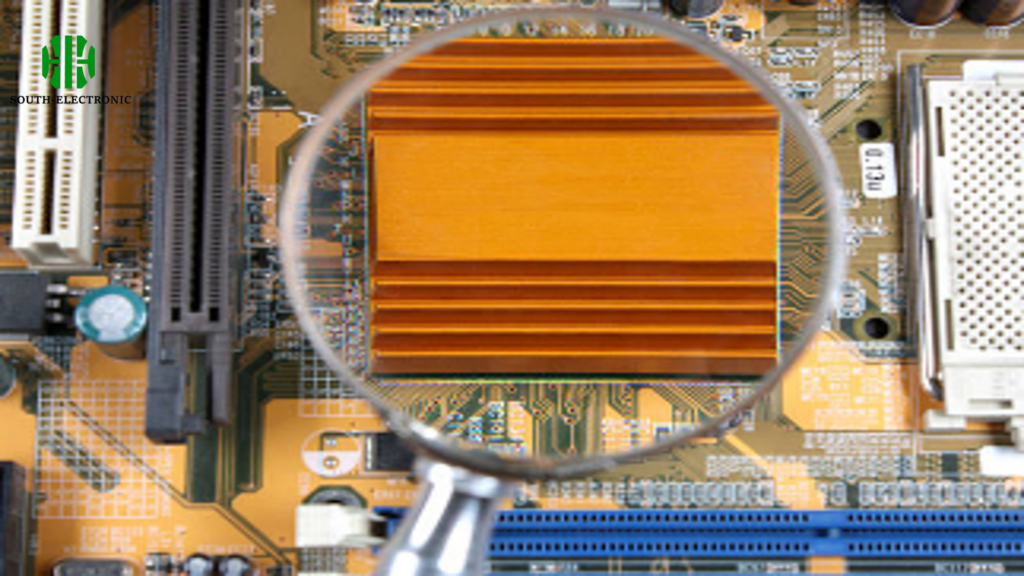
What exactly is PCB lamination? In essence, it's a sophisticated method of constructing Printed Circuit Boards (PCBs) by layering and fusing various components together. PCB laminates are created by gluing layers together. Traditionally, a PCB consists of four layers: substrate, copper, solder mask, and screen printing (from bottom to top). Laminates are developed using thermosetting resins that cure under the pressure and temperature of the fabric to form a final part of uniform thickness.
Importance
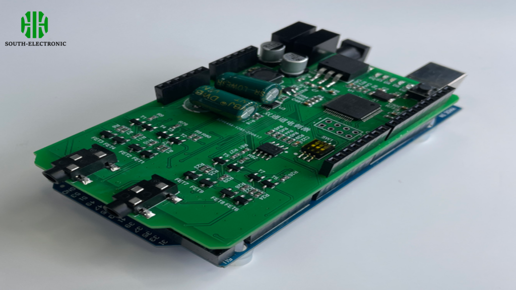
Well-laminated PCB guarantees not only structural sturdiness but also electrical reliability. It ensures that the board can withstand various operational stresses, such as thermal fluctuations, without falling apart or malfunctioning. Moreover, in the intricate world of multi-layer PCBs, where layers are stacked like a high-tech sandwich, precision lamination becomes even more crucial. It's about achieving that perfect balance between compactness and enhanced electrical properties, meeting the high demands of modern technology.
Base materials
FR4: This is like the industry standard, a fiberglass-reinforced epoxy laminate. It's renowned for its excellent balance of strength, affordability, and electrical insulation properties. It's like the all-rounder in PCB laminates, suitable for a vast array of applications.
High-frequency laminate: Commonly used in advanced communications systems and radar technology. This is where materials like Rogers and Teflon come into play. They were chosen for their low electrical losses and stable performance at higher frequencies, making them ideal for applications where accuracy is critical.
Polyimide laminates: They are like the endurance athletes of laminates, able to withstand high temperatures and harsh environments, making them ideal for aerospace and military applications.
CEM laminate: It is a mixture of cellulose paper and fiberglass fabric. They are somewhat of a middle ground, offering better performance than the FR4 in some aspects but still maintaining a reasonable cost.
PCB Lamination Technology
Vacuum Lamination: This technology is all about precision. By eliminating air, we ensure an even bond without any nasty voids or air pockets that could compromise the integrity of the PCB. It is particularly suitable for high-rise count PCBs where uniform distribution is critical.
Pressure Lamination: It relies on the application of direct pressure to fuse the PCB layers together. It is the workhorse of lamination technology and is widely used for its robustness and reliability. This approach is somewhat of a reliable backbone for PCB lamination, providing a solid combination of efficiency and cost-effectiveness for a wide range of applications.
Thermal Lamination: This method brings heat into the equation, ensuring the prepreg material flows and solidifies evenly by applying controlled thermal energy, creating a strong bond between the layers. It's akin to a carefully choreographed thermal ballet and is critical to achieving perfect layers in complex PCBs.
Comparing these technologies, each has its own merits. Vacuum lamination is the first choice for high-precision and complex circuit boards, despite the higher cost. Pressure lamination is a reliable, cost-effective solution for a variety of standard PCBs. There's also thermal lamination, which is your choice when you need the perfect combination of heat and pressure to achieve intricate layering.
Conclusion
PCB lamination technology is a testament to the blend of science and engineering. Its evolution is not just a response to current demands but a stepping stone to future innovations. As we embrace an increasingly digital world, the role of advanced PCB lamination technology becomes more crucial, paving the way for the next generation of electronic devices.


