

Ever wondered why smartphones never melt during charging? The secret lies in reflow soldering[^1]'s surgical precision - a process I've witnessed make or break $50k PCB batches. This invisible thermal dance determines every modern device's reliability.
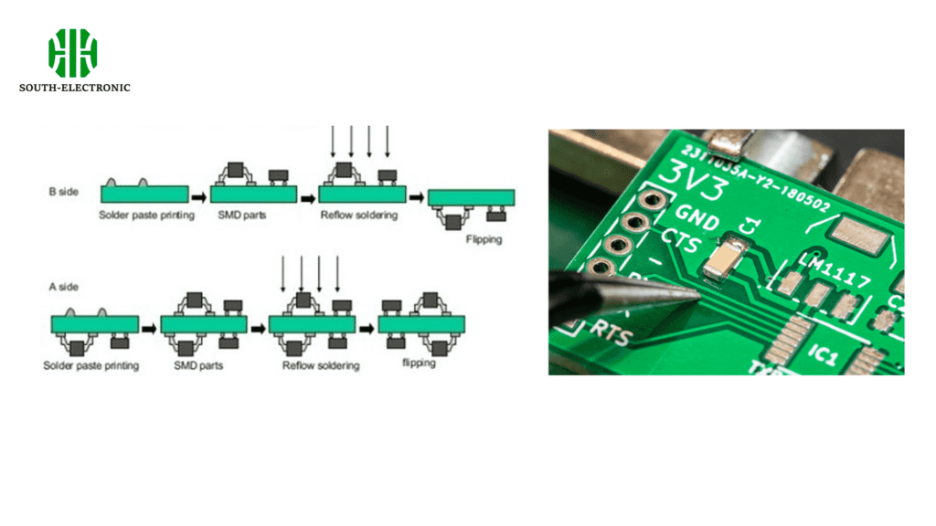
Reflow soldering bonds components to PCBs using precisely controlled heat phases (preheat/soak/reflow/cool), transforming solder paste into permanent metallic connections. Advanced systems now use nitrogen environments[^2] to prevent oxidation, achieving near-zero defect rates in automotive and IoT devices.
While reflow seems simple, its chemical complexities separate hobbyist tinkering from military-grade electronics. Let's dissect the critical stages, troubleshoot common failures, and explore bleeding-edge IoT/5G applications.
The 5-Stage Reflow Soldering Process Demystified
Watch new engineers panic when solder balls form - usually from skipping the thermal soak stage[^3] I strictly enforce in aerospace projects. Every phase serves non-negotiable chemical purposes:
The process flows: preheating (20-100°C/sec) removes solvents, thermal soaking (60-120sec) activates flux, reflow (220-250°C) melts alloy particles, and controlled cooling (2-5°C/sec) creates durable intermetallic bonds. Modern systems add nitrogen purging to block oxygen contamination.
Phase Breakdown With Critical Parameters
| Stage | Temp Range | Duration | Key Chemical Reactions |
|---|---|---|---|
| Preheat | 25°C→150°C | 2-3 min | Solvent evaporation |
| Soak | 150°C→180°C | 60-90 sec | Flux activation, thermal equalization |
| Reflow Spike | 180°C→220°C | 45-60 sec | Sintering of alloy particles |
| Peak | 220°C→245°C | 40-50 sec | Full intermetallic bond formation[^4] |
| Cooling | 245°C→50°C | 3-4 min | Microstructure stabilization |
Never rush cooling - forced air cooling creates brittle joints that fail in thermal cycling tests. I specify programmable liquid cooling[^5] for medical devices needing 20-year reliability.
Why Thermal Profiling Is the Heart of Successful Reflow?
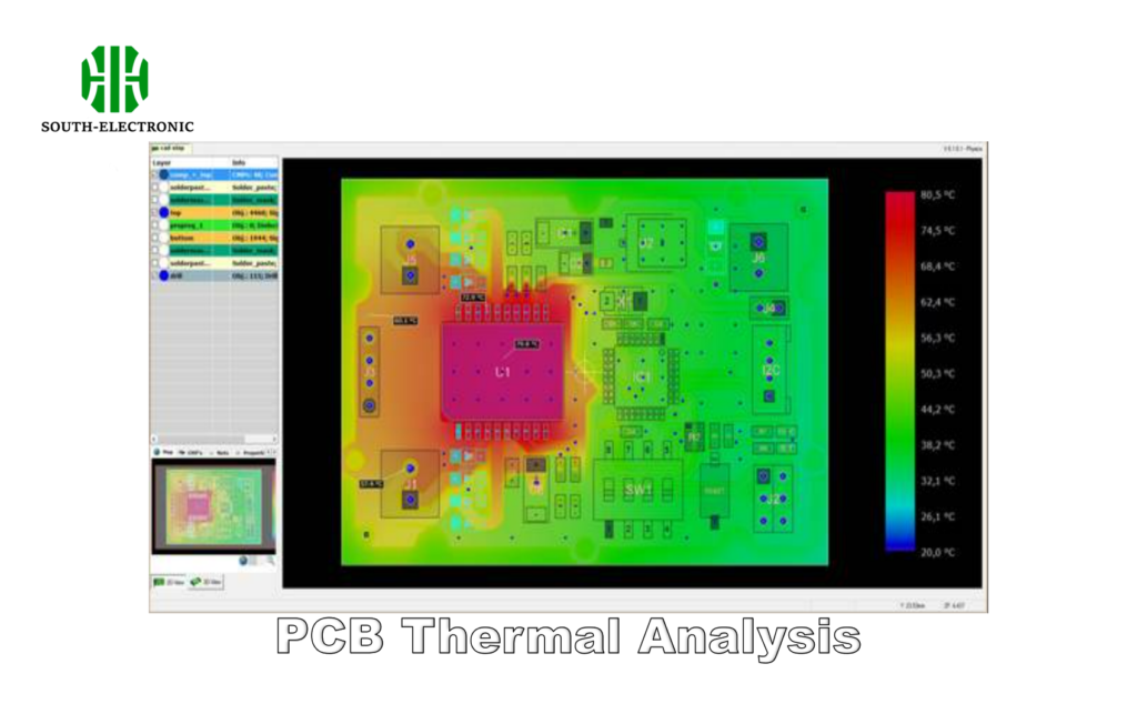
When a batch of automotive ECUs failed at -40°C testing, we discovered the profile's peak was 8°C too low - the difference between reliable connections and latent defects.
Thermal profiling[^6] ensures uniform heat distribution to activate flux, melt solder, and form proper intermetallic layers. Advanced systems now use real-time IR sensors and AI to adjust conveyor speed based on component mass variations.
)
Key Profile Parameters by Product Type
| Device Class | Soak Time | Peak Temp | Cooling Rate | Nitrogen Level |
|---|---|---|---|---|
| Consumer PCB | 70 sec | 235°C | 3°C/sec | <500ppm O₂ |
| Automotive | 90 sec | 245°C | 2°C/sec | <100ppm O₂ |
| Medical | 110 sec | 240°C | 1.5°C/sec | <50ppm O₂ |
| Military | 120 sec | 250°C | 2.5°C/sec | <20ppm O₂ |
Always verify profiles with K-type thermocouples - IR sensors can misread reflective surfaces. I log 3D thermal maps[^7] for mission-critical boards.
How to Diagnose 7 Common Reflow Defects?
A client once had 30% boards with head-in-pillow defects[^8] - turned out their moisture-sensitive BGAs[^9] absorbed humidity during storage. Simple vacuum packing solved their $2M recall risk.
Top defects: solder balls (ramp rate too fast), tombstoning (imbalanced pads), voids (contaminated paste), cold joints (insufficient peak time), bridging (excessive paste), head-in-pillow (oxidized pads), and graping (multiple reflows).
)
Defect Matrix and Correction Tactics
| Failure Mode | Visual Signs | Root Cause | Corrective Action |
|---|---|---|---|
| Solder Balls | Metal spheres around pads | Rapid preheating | Reduce initial ramp rate <3°C/sec |
| Tombstoning | Vertical components | Uneven thermal mass | Redesign pad symmetry |
| Voiding | X-ray visible pores | Moisture in paste | Use N₂ purged storage |
| Cold Joints | Dull grainy surfaces | Peak temp too low | Increase to 245°C+ |
| Bridging | Solder connects adjacent leads | Stencil alignment issues | Implement laser-cut stencils |
| Head-in-Pillow | Ball/pad separation | Component oxidation | Use flux-cored solder balls |
| Graping | Clustered solder spheres | Multiple reflows | Limit to 2 reflow cycles |
Always maintain SPC charts for paste viscosity and stencil alignment - most defects trace back to process control lapses.
Future-Proofing Your Process: Adaptive Reflow for IoT/5G PCBs[^10]
Recent mmWave antenna modules demanded a hybrid vapor phase/reflow approach[^11] I developed - traditional methods couldn't handle 0.3mm pitch arrays without warping.
Next-gen reflow combines liquid metal cooling zones, inline AOI feedback loops, and ML-driven predictive adjustments. For 5G FR2 boards, we're testing laser-assisted local heating[^12] to protect temperature-sensitive components.
Emerging Techniques Comparison
| Technology | Resolution | Energy Use | Best For | Industry Adoption |
|---|---|---|---|---|
| Convection Reflow | ±5°C | 15kW | Standard SMT | 85% market |
| Vapor Phase | ±1.5°C | 8kW | High-density PCBs | Growing in medical |
| Laser Local | ±0.3°C | 3kW | Mixed alloy assemblies | R&D phase |
| Induction Heating | ±2°C | 12kW | Thick boards | Automotive trials |
| Resistance Heating | ±4°C | 10kW | Low-cost consumer | Phasing out |
Consider modular systems - our hybrid convection/laser line handles everything from flex PCBs to ceramic substrates without retooling costs.
Conclusion
Mastering reflow requires understanding metallurgical transformations, not just oven settings. With thermal profiling and defect prevention strategies, manufacturers achieve Six Sigma yields - even in cutting-edge 5G/IoT applications.
[^1]: Understanding reflow soldering is crucial for anyone interested in electronics manufacturing. This resource will provide in-depth insights into the process.
[^2]: Nitrogen environments are key to achieving high-quality solder joints. Discover how they prevent oxidation and enhance reliability.
[^3]: The thermal soak stage is vital for ensuring quality in soldering. Explore this link to learn why skipping it can lead to failures.
[^4]: Intermetallic bonds are vital for strong solder joints. Learn more about their formation and impact on reliability in electronics.
[^5]: Programmable liquid cooling can significantly enhance the reliability of medical devices. Discover its advantages and applications in this informative link.
[^6]: Understanding thermal profiling is crucial for ensuring reliable solder connections in electronics manufacturing. Explore this resource to enhance your knowledge.
[^7]: Explore the importance of 3D thermal maps for accurate diagnostics and improving PCB performance.
[^8]: Understanding head-in-pillow defects can help you prevent costly recalls and improve product quality.
[^9]: Learn about moisture-sensitive BGAs to enhance your PCB design and avoid reliability issues.
[^10]: Explore this link to understand how adaptive reflow techniques are revolutionizing PCB manufacturing for IoT and 5G applications.
[^11]: Learn about the innovative hybrid vapor phase/reflow approach that addresses challenges in high-density PCB assembly.
[^12]: Discover the benefits of laser-assisted local heating in protecting temperature-sensitive components during PCB assembly.


