
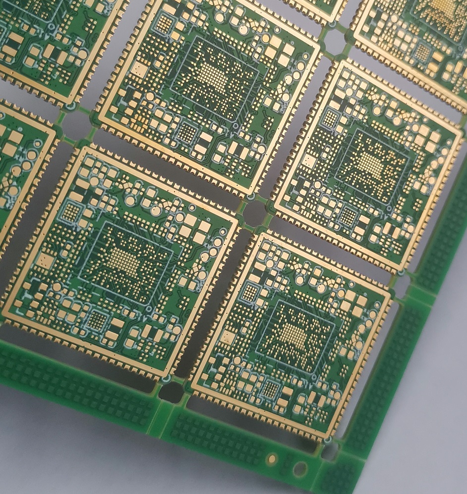
Service de conception de PCB HDI
South-Electronic
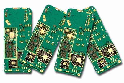
Chez South-Electronic, nous disposons de la technologie avancée de connexion à haute densité (HDI) pour garantir que chaque conception de PCB que nous réalisons est aussi précise et efficace que possible. Si vous voulez que votre PCB soit fiable et performant, nos PCB HDI sont ce qu'il vous faut.
Pourquoi choisir South-Electronic ?
-
Conception personnalisée
Conception personnalisée pour répondre à vos besoins uniques.
Chez South-Electronic, nous comprenons que chaque projet est unique. C'est pourquoi nos services de conception de PCB sont personnalisés pour répondre à vos exigences spécifiques, garantissant que chaque détail est exécuté selon vos spécifications exactes. Cela améliorera la performance et la fiabilité de vos produits. -
Satisfaction garantie
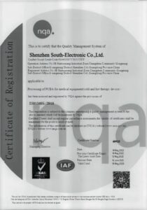
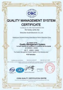
Vous apprécierez la confiance de travailler avec une entreprise certifiée ISO9001.
Nous privilégions une communication claire et transparente et nous nous engageons à respecter les normes les plus élevées, garantissant que vos PCB non seulement répondent mais dépassent vos attentes en matière de performance, de durabilité et de précision. -
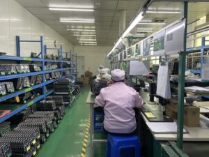
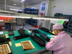
Service tout-en-un
Lorsque vous nous choisissez, vous obtenez une solution complète pour vos PCB, de la conception et du prototypage à la production en série.
Nous offrons un service tout-en-un, éliminant la complexité et le coût de la gestion de plusieurs fournisseurs. -
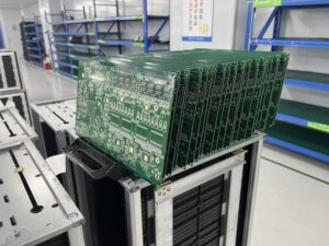
Service complet
Vous bénéficiez d'une satisfaction totale grâce à notre large gamme d'équipements.
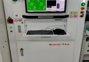
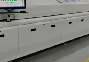
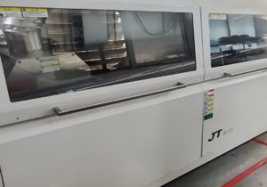
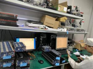
Nous disposons d'une vaste gamme de capacités de traitement de PCB. De la conception à la livraison, nous avons les équipements et les processus pour garantir que votre commande est correctement réalisée. -
Livraison rapide
Vous respectez vos délais grâce à nos délais d'exécution rapides.
Notre production rationalisée garantit des délais d'exécution rapides, pour que vous receviez vos produits quand vous en avez besoin, sans retard.
Projets connexes que nous avons réalisés
Avis des clients
Questions fréquentes
Questions les plus posées
Envoyez-nous un message
Plus vous remplissez de détails, plus nous pourrons avancer rapidement à l’étape suivante.


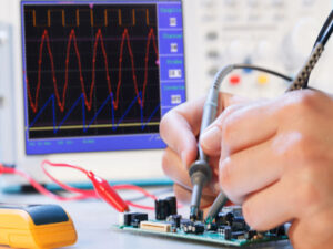


Le guide complet pour la conception de PCB HDI
Sommaire
Chapitre 1
Introduction à la conception de PCB HDI
Vue d’ensemble de la technologie HDI dans les PCB
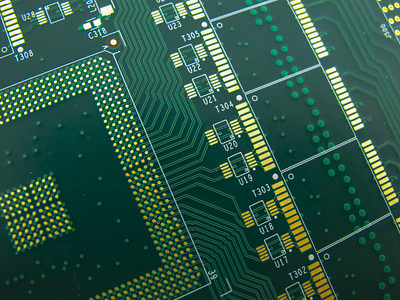
La technologie de connexion à haute densité (HDI) est une révolution dans le domaine de la conception des circuits imprimés (PCB). Elle permet d’intégrer plus de composants dans un espace plus réduit que jamais auparavant. Comment ? En utilisant des lignes plus fines, des vias plus petits et en rapprochant les composants. Comprendre la technologie HDI vous aidera à concevoir des dispositifs plus petits, plus efficaces et plus performants lorsque vous vous aventurez dans le monde de l’électronique. Les PCB HDI utilisent des techniques avancées telles que les microvias, les cartes multicouches construites en couches successives et l’intégrité des signaux haute fréquence pour repousser les capacités de votre produit au-delà des limites des conceptions traditionnelles.
Importance et évolution des PCB HDI dans l’électronique moderne
Les PCB HDI jouent un rôle crucial dans l’industrie électronique d’aujourd’hui. À mesure que les dispositifs deviennent plus petits et plus complexes, la demande pour des cartes pouvant supporter une haute densité de composants sans compromettre les performances augmente. La technologie HDI a relevé ce défi. Elle est passée d’un moyen d’améliorer l’apparence et la fonctionnalité des appareils électroniques grand public à une composante essentielle dans des applications de haute importance telles que les dispositifs médicaux, les systèmes automobiles et l’ingénierie aérospatiale. Cela est dû aux progrès constants dans les techniques de fabrication et la science des matériaux, ce qui signifie que vous pouvez continuer à repousser les limites du possible dans vos conceptions électroniques.
Termes clés et définitions
En travaillant avec les PCB HDI, connaître ces termes clés vous aidera à comprendre et à maîtriser rapidement le domaine :
- Microvias : Petits trous percés au laser pour connecter différentes couches d’un PCB, essentiels pour économiser de l’espace et améliorer les performances des PCB HDI.
- Cartes multicouches construites en couches (Build-up Multilayer Boards) : Une méthode où des couches supplémentaires sont ajoutées séquentiellement aux couches de cuivre de base, permettant une conception de carte plus compacte.
- Intégrité du signal (Signal Integrity) : La mesure de la qualité d’un signal électrique, primordiale dans les PCB HDI pour garantir la fonctionnalité et les performances.
- Densité des pads (Pad Density) : Se réfère au nombre de points de connexion par unité de surface sur une carte, généralement plus élevé dans les PCB HDI par rapport aux cartes conventionnelles.
Chapitre 2
Avantages des PCB HDI
Performances électriques améliorées
En choisissant des PCB HDI, vous optez pour des performances électriques supérieures, essentielles pour les appareils électroniques à haute vitesse d’aujourd’hui. L’utilisation des microvias et des interconnexions densément regroupées dans les PCB HDI réduit les chemins électriques, minimise les interférences et améliore l’intégrité des signaux. Cela signifie que vous pouvez vous attendre à des taux de transmission des signaux plus rapides et à une meilleure fiabilité dans le fonctionnement de vos appareils électroniques. Que vous conceviez pour l’électronique grand public, les télécommunications ou les applications à haute fréquence, les PCB HDI offrent les améliorations de performance dont vous avez besoin pour rester compétitif.
Densité accrue des circuits et ses avantages
La caractéristique principale de la technologie HDI est sa capacité à augmenter la densité des circuits. Cela signifie davantage de fonctionnalités dans un espace plus réduit, un avantage essentiel alors que les appareils électroniques deviennent plus petits et plus complexes. Pour vous, cela se traduit par la possibilité de concevoir des appareils plus compacts sans compromettre les performances—comme les smartphones, les montres connectées et les implants médicaux. La densité accrue des circuits facilite également une meilleure gestion thermique et une efficacité énergétique, qui sont cruciales pour la fiabilité et la durabilité à long terme de vos produits.
Fiabilité et durabilité dans les environnements exigeants
En choisissant des PCB HDI, vous investissez dans la fiabilité et la durabilité, particulièrement importantes dans des environnements difficiles tels que l’automobile, l’aérospatiale et l’électronique industrielle. Les PCB HDI sont conçus pour être robustes, avec une sélection avancée des matériaux et des techniques de superposition innovantes qui leur permettent de résister à des conditions difficiles telles que des températures élevées, des vibrations et l’humidité. Cette durabilité prolonge non seulement la durée de vie des composants électroniques, mais garantit également des performances constantes sous contrainte, vous offrant la confiance que votre produit fonctionnera comme prévu, quelles que soient les conditions.
En résumé, les PCB HDI vous offrent un triple avantage : des performances électriques inégalées, une densité de circuits accrue pour la miniaturisation et une fiabilité et une durabilité exceptionnelles. Ces avantages sont indispensables dans le paysage technologique actuel en constante évolution, où les exigences sur les appareils électroniques sont plus grandes que jamais. En intégrant les PCB HDI dans vos conceptions, vous ne faites pas que suivre les normes de l’industrie—vous les définissez.
Chapitre 3
Design Considerations for HDI PCBs
Choix des matériaux pour les PCB HDI
Les matériaux que vous sélectionnez influencent directement les performances et la fiabilité de vos appareils électroniques. Vous devez choisir des matériaux de substrat qui prennent en charge la gravure de lignes fines et offrent une excellente stabilité thermique et une faible perte diélectrique, en particulier pour les applications à haute fréquence. Des matériaux haute performance tels que le FR-4 à TG élevé, le polyimide et la résine BT sont des choix populaires qui répondent à ces besoins. Chaque matériau offre différents avantages, tels qu’une meilleure résistance à la chaleur ou des propriétés mécaniques améliorées, vous permettant d’adapter le PCB aux exigences spécifiques de votre projet. En choisissant les bons matériaux, vous vous assurez que vos PCB HDI peuvent prendre en charge des dispositions de composants denses et sont suffisamment durables pour relever les défis opérationnels auxquels ils seront confrontés.
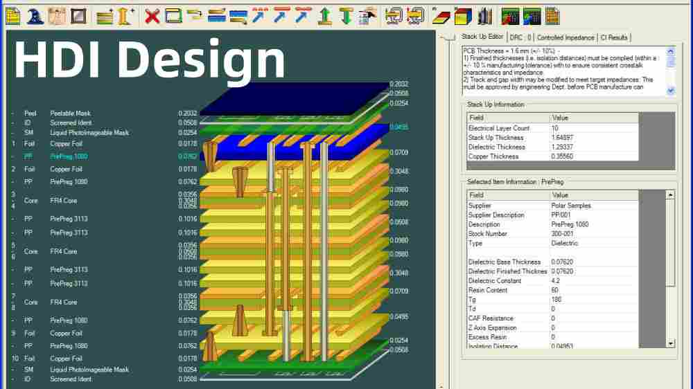
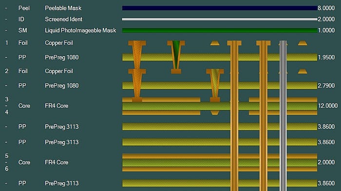
Configuration des couches et considérations d’empilement
La configuration des couches et leur empilement sont essentiels pour maximiser les avantages de la technologie HDI. Lorsque vous concevez votre PCB HDI, considérez comment l’agencement des couches peut affecter à la fois les performances électriques et la fabricabilité de la carte. Une configuration des couches appropriée peut réduire les problèmes d’intégrité des signaux en minimisant les distances que les signaux doivent parcourir entre les composants, réduisant ainsi les retards et les interférences potentiels. Un empilement bien planifié peut également améliorer la gestion thermique de la carte, ce qui est crucial pour les circuits à haute densité. Les configurations courantes incluent l’utilisation de vias enterrés et de conceptions Via-in-Pad pour libérer de l’espace en surface pour des composants supplémentaires. Ce stratagème de superposition optimise non seulement les performances électriques mais contribue également à la miniaturisation du dispositif, vous permettant de repousser les limites de ce que vos produits peuvent accomplir.
Types de vias utilisés dans les PCB HDI
Les vias sont un composant fondamental des PCB HDI et jouent un rôle essentiel dans l’interconnexion entre les couches. Comprendre les types de vias disponibles et savoir les utiliser efficacement est essentiel à votre processus de conception. Les microvias, qui sont des vias de petit diamètre percés au laser, sont une caractéristique clé de la conception HDI. Ils permettent un routage à très haute densité mais ne peuvent être utilisés que pour quelques couches. Les vias enterrés, cachés dans le PCB, et les vias borgnes, qui connectent une couche externe à une ou plusieurs couches internes, aident à réaliser des conceptions plus compactes et plus efficaces. En utilisant efficacement ces différents types de vias, vous pouvez améliorer considérablement les performances de vos PCB HDI en minimisant la longueur des chemins pour les signaux électriques et en optimisant l’espace disponible sur chaque couche.
En réfléchissant soigneusement au choix des matériaux, à la configuration des couches et aux types de vias, vous vous assurez que vos PCB HDI sont à la pointe de la technologie et offrent la robustesse et l’efficacité nécessaires pour répondre aux exigences technologiques actuelles. En vous concentrant sur ces aspects clés, vous positionnez vos produits électroniques pour exceller en termes de performances et de fiabilité.
Chapitre 4
Processus de conception des PCB HDI
Guide étape par étape, de la conceptualisation au design final
La conception d’un PCB HDI commence par votre vision. Vous devez imaginer ce que vous voulez que votre appareil électronique fasse et ce qu’il doit pouvoir accomplir. Voici les étapes du processus de conception :
- Analyse des besoins : Commencez par définir les exigences de performance, les contraintes de taille et les conditions environnementales que votre PCB doit supporter. Comprendre ces aspects dictera les complexités du schéma et de la fabrication.
- Conception du schéma : Ensuite, créez un diagramme schématique détaillé représentant toutes les connexions électriques entre les composants. Cette étape critique vous permet de cartographier votre circuit et de prendre des décisions sur le placement des composants, ce qui influence considérablement les performances et la fabricabilité de votre PCB HDI.
- Disposition de la carte : Avec votre schéma en main, commencez la disposition. À ce stade, le placement des composants et le routage des traces sont réalisés selon les directives HDI pour optimiser l’espace et améliorer l’intégrité des signaux.
- Planification de l’empilement des couches : Décidez du nombre de couches et de leur disposition en fonction de la complexité du circuit et des besoins en intégrité de puissance. Cela inclut le choix du type de vias (microvias, vias enterrés) pour interconnecter les couches efficacement.
- Simulation et tests : Avant de finaliser le design, effectuez des simulations pour vérifier les performances électriques, y compris l’intégrité des signaux et les caractéristiques thermiques. Résolvez tout problème identifié pour éviter des révisions coûteuses ultérieures.
- Fabrication de prototype : Une fois le design finalisé, fabriquez un prototype pour tester physiquement la conception. Cette étape nécessite souvent des ajustements en fonction des performances du prototype.
- Itération finale et production : Après des tests approfondis et des ajustements, finalisez votre conception pour la production en série. Assurez-vous que toutes les spécifications sont respectées pour offrir des performances optimales dans les applications prévues.
Outils et logiciels recommandés pour la conception des PCB HDI
Une conception efficace des PCB HDI nécessite des outils sophistiqués capables de gérer les complexités des agencements haute densité :
- Logiciels de conception assistée par ordinateur (CAD) : Utilisez des logiciels CAD avancés comme Altium Designer, Cadence Allegro, ou Mentor Graphics PADS pour un travail précis et détaillé. Ces outils offrent des fonctionnalités robustes pour la gestion des couches, le routage automatique et la visualisation 3D de l’empilement de votre PCB.
- Logiciels de simulation : Des outils comme ANSYS ou HyperLynx sont indispensables pour l’analyse de l’intégrité des signaux et des performances thermiques, permettant d’anticiper et de résoudre les problèmes avant le développement des prototypes physiques.
Conseils pour une capture schématique et une planification d’agencement efficaces
- Gardez les composants proches : Placez les composants connexes à proximité pour minimiser les longueurs des traces, ce qui réduit la dégradation et les interférences des signaux.
- Exploitez les techniques HDI : Utilisez pleinement les microvias et les technologies Via-in-Pad pour maximiser l’espace et améliorer les performances de vos PCB.
- Prévoyez la dissipation thermique : Considérez les chemins thermiques dans votre conception pour une gestion efficace de la chaleur, en particulier dans les cartes à haute densité.
- Testez régulièrement : Intégrez des tests à chaque étape du processus de conception. La détection précoce des problèmes peut économiser un temps et des ressources considérables.
En suivant ces étapes et en utilisant les bons outils, vous pouvez naviguer efficacement dans les complexités de la conception des PCB HDI, garantissant que votre produit final dépasse les attentes. Ce processus nécessite non seulement des compétences techniques, mais aussi une approche visionnaire pour intégrer forme, fonctionnalité et préparation au futur dans vos produits électroniques.
Chapitre 5
Techniques de fabrication des PCB HDI
Aperçu des processus de fabrication uniques aux PCB HDI
La fabrication des PCB à haute densité d’interconnexion (HDI) implique des techniques sophistiquées répondant à leurs exigences uniques en termes de densité élevée de composants et de lignes plus fines. En vous lançant dans la fabrication de ces cartes avancées, vous rencontrerez des processus tels que la formation de microvias, la stratification séquentielle et le perçage laser direct, essentiels pour obtenir les conceptions compactes et efficaces caractéristiques de la technologie HDI. Ces processus sont conçus pour réduire le nombre de couches tout en augmentant la fonctionnalité, ce qui est crucial pour les appareils électroniques modernes exigeant une taille minimale sans compromettre les performances.
Principaux défis de fabrication et solutions
La fabrication des PCB HDI présente plusieurs défis, mais avec les bonnes stratégies, ils peuvent être surmontés efficacement :
- Formation des microvias : L’un des plus grands défis est la formation des microvias, ces petits trous percés dans le PCB pour connecter différentes couches. Cela nécessite un contrôle précis pour éviter des défauts tels que le perçage incomplet ou des vides dans le placage. L’utilisation d’équipements de perçage laser avancés garantit précision et cohérence dans la formation des microvias.
- Alignement des couches : À mesure que le nombre de couches augmente, maintenir un alignement parfait devient crucial et difficile. Un mauvais alignement peut entraîner des échecs de connexion et une fiabilité réduite. L’utilisation de méthodes d’inspection optique pendant le processus de stratification peut garantir que chaque couche est correctement alignée.
- Intégrité des signaux : Maintenir l’intégrité des signaux dans des circuits densément emballés est essentiel. L’utilisation d’outils de simulation pendant la phase de conception peut prédire les problèmes potentiels dus aux interactions de signaux. De plus, une planification minutieuse du routage des traces et des techniques de blindage pendant la fabrication peut atténuer ces effets.
Équipements et technologies utilisés dans la production
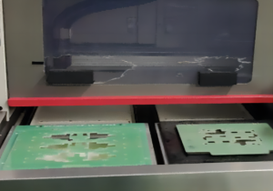
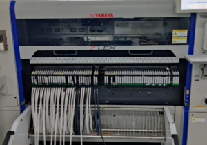
Pour répondre aux exigences de fabrication des PCB HDI, votre installation doit être équipée de technologies de pointe :
- Machines de perçage laser : Essentielles pour créer des microvias, les machines de perçage laser permettent une grande précision et un contrôle, idéales pour les petites dimensions requises dans les PCB HDI.
- Systèmes d’inspection optique automatisée (AOI) : Ces systèmes sont cruciaux pour garantir que chaque couche du PCB est exempte de défauts et correctement alignée avant de passer à l’étape suivante du processus de fabrication.
- Équipements de placage électrolytique : Un placage approprié des vias et des traces est vital pour le bon fonctionnement des PCB HDI. Les systèmes modernes de placage électrolytique offrent le contrôle nécessaire pour obtenir un placage cohérent et fiable, notamment dans le cas des microvias et des traces fines.
- Presses de stratification séquentielle : Utilisées pour lier plusieurs couches de PCB HDI sous une température et une pression contrôlées, ces presses garantissent une adhérence solide et un enregistrement précis des couches.
En maîtrisant ces techniques et en utilisant les équipements appropriés, vous pouvez garantir la production de PCB HDI de haute qualité répondant aux normes exigeantes des applications électroniques avancées. Cela renforcera non seulement la fiabilité et les performances des produits que vous créez, mais positionnera également vos opérations de fabrication à la pointe de l’industrie électronique.
Chapitre 6
Tests et assurance qualité pour les PCB HDI
Méthodes de test courantes
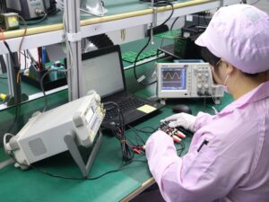
Pour garantir que vos PCB HDI fonctionnent de manière fiable dans toutes les conditions, une suite complète de tests est essentielle. Voici les principales méthodes de test à mettre en œuvre :
- Test électrique : Cela consiste à vérifier les courts-circuits, les circuits ouverts et les valeurs d’impédance correctes pour assurer la fonctionnalité électrique. Avec un testeur Flying Probe ou Bed of Nails, vous pouvez effectuer ces tests rapidement et efficacement sans avoir besoin d’un contact direct avec chaque composant du circuit, idéal pour les conceptions denses des PCB HDI.
- Test thermique : Compte tenu de la nature compacte des PCB HDI, la gestion thermique est cruciale. Les tests thermiques permettent de vérifier que vos cartes peuvent fonctionner efficacement dans diverses conditions thermiques sans dégradation des performances. Des techniques telles que les tests de cycle thermique, où le PCB est soumis à des températures variables pour simuler les environnements opérationnels, sont couramment utilisées.
- Test de l’intégrité des signaux : À mesure que les fréquences augmentent, maintenir l’intégrité des signaux devient plus difficile. Les tests d’intégrité des signaux garantissent que le PCB peut transmettre des signaux sans distorsion ou perte excessive, essentiel pour les applications à haute vitesse.
Normes de qualité applicables aux PCB HDI
Adhérer aux normes de qualité reconnues ne se limite pas à la conformité ; c’est garantir la longévité et la fiabilité de vos PCB HDI. Voici quelques normes à considérer :
- IPC-6012 : Cette norme régit les spécifications de qualification et de performance pour les cartes rigides imprimées, y compris celles utilisées dans les conceptions HDI. Respecter l’IPC-6012 garantit que vos PCB répondent à des exigences rigoureuses de fiabilité et de qualité.
- ISO 9001 : Bien qu’elle ne soit pas spécifique aux PCB, la certification ISO 9001 dans vos processus de fabrication garantit que vous disposez d’un système de gestion de la qualité robuste, conduisant à une plus grande cohérence et satisfaction client.
- IPC-A-600 : Connu sous le nom de « Acceptabilité des cartes imprimées », cette norme aide à évaluer visuellement la qualité des PCB, en se concentrant sur des critères tels que la qualité des matériaux, les conditions de surface et la qualité des trous, essentiels pour les PCB HDI.
Manipulation et inspection pendant le processus de QA
La manipulation et l’inspection sont des étapes cruciales du processus d’assurance qualité, en particulier pour les PCB HDI où même de petites imperfections peuvent entraîner des problèmes significatifs :
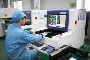
- Inspection optique automatisée (AOI) : Avant et après l’assemblage, utilisez des systèmes AOI pour vérifier les défauts de surface tels que les rayures ou les erreurs de gravure. Cette méthode est particulièrement efficace aux premières étapes pour empêcher les cartes défectueuses de progresser dans le processus de production.
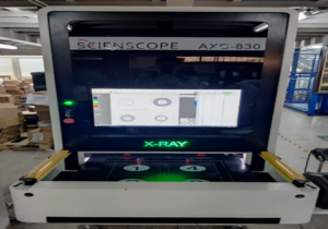
- Inspection aux rayons X : Elle est cruciale pour inspecter les microvias et autres caractéristiques cachées invisibles à l’œil nu. L’inspection aux rayons X permet de vérifier l’intégrité des couches internes et des interconnexions, garantissant qu’elles sont exemptes de défauts tels que des vides ou des mauvais alignements.
- Inspection manuelle : Bien que les méthodes automatisées soient efficaces, les inspections manuelles par du personnel qualifié peuvent être inestimables, en particulier pour les vérifications finales. Cela permet d’identifier des problèmes que les machines pourraient manquer et ajoute une couche supplémentaire d’assurance avant l’expédition de votre produit.
En mettant en œuvre ces méthodes de test et en respectant des normes de qualité rigoureuses, vous fournissez à vos clients des PCB HDI qui non seulement répondent mais dépassent leurs attentes en termes de performances et de fiabilité. Cet engagement envers l’assurance qualité est ce qui vous distingue dans le paysage compétitif de la fabrication électronique.
Chapitre 7

Applications des PCB HDI
Cas d’utilisation dans diverses industries
Les PCB HDI sont essentiels dans de nombreuses industries, chacune tirant parti des capacités uniques de ces solutions d’interconnexion à haute densité :
- Automobile : Dans le secteur automobile, les PCB HDI sont cruciaux pour prendre en charge l’électronique avancée des véhicules modernes. Des systèmes d’infodivertissement aux fonctionnalités de sécurité telles que les contrôleurs d’airbags et les systèmes de freinage antiblocage, les PCB HDI offrent la fiabilité et les performances nécessaires dans des environnements soumis à des vibrations et des températures extrêmes.
- Aérospatiale : Les applications aérospatiales exigent une fiabilité et une précision maximales, et les PCB HDI répondent à ces attentes. Ils sont utilisés dans les instruments de cockpit, les systèmes de communication et la navigation par satellite, où leur capacité à gérer des signaux haute fréquence est indispensable.
- Électronique grand public : Dans l’électronique grand public, les PCB HDI permettent la miniaturisation des appareils tels que les smartphones, les tablettes et les appareils portables. Ils permettent d’intégrer davantage de fonctions dans des espaces plus restreints sans compromettre les performances, aboutissant à des appareils plus élégants et plus performants.
- Dispositifs médicaux : Les PCB HDI sont également largement utilisés dans les équipements médicaux, y compris les systèmes d’imagerie et les instruments de diagnostic portables. Leur haute fiabilité et leur petite taille les rendent idéaux pour des applications médicales critiques où la précision et la durabilité sont essentielles.
Études de cas illustrant l’impact des PCB HDI
- Innovation dans les smartphones : Un fabricant de smartphones de premier plan a utilisé des PCB HDI pour révolutionner son dernier modèle. En intégrant la technologie HDI, ils ont réussi à doubler la durée de vie de la batterie et à améliorer les fonctionnalités de l’appareil photo sans augmenter la taille du téléphone, offrant aux consommateurs un appareil beaucoup plus robuste.
- Améliorations de la sécurité automobile : Une entreprise automobile a intégré des PCB HDI dans ses systèmes de sécurité, améliorant considérablement la réactivité et la fiabilité des fonctionnalités d’urgence de ses véhicules. Cette innovation a contribué à une meilleure notation en matière de sécurité, renforçant ainsi la confiance des clients et augmentant les ventes.
Tendances futures des applications
L’avenir des PCB HDI promet des applications et des innovations encore plus larges :
- Internet des objets (IoT) : À mesure que les appareils IoT deviennent plus répandus, la demande pour des PCB petits et performants augmentera. Les PCB HDI sont parfaitement adaptés pour répondre à ces besoins, permettant de connecter plusieurs capteurs et actionneurs dans des espaces compacts.
- Technologie portable : L’industrie de la technologie portable est en pleine expansion, et les PCB HDI en sont au cœur. Leur capacité à s’adapter à des espaces petits, parfois irréguliers, tout en maintenant leur fonctionnalité, les rend idéaux pour cette application.
- Intelligence artificielle (IA) : À mesure que l’IA évolue, l’électronique qui la soutient doit gérer des quantités croissantes de données à des vitesses plus élevées. Les PCB HDI, avec leur excellente intégrité des signaux et leurs capacités de densité, sont essentiels pour rendre l’IA plus accessible dans les appareils du quotidien.
En intégrant les PCB HDI dans vos produits, vous ne faites pas que suivre les tendances technologiques actuelles ; vous les devancez, prêt à relever les défis du paysage électronique de demain. Cet engagement envers l’innovation garantit que vos conceptions continueront à repousser les limites du possible, ayant un impact significatif dans diverses industries.
Chapitre 8
Défis et solutions dans la conception des PCB HDI
Résolution des problèmes d’intégrité du signal
L’intégrité du signal est une préoccupation primordiale dans la conception des PCB HDI en raison de leur haute densité et de leur compacité. Lors de la conception impliquant des signaux à haute vitesse, vous pouvez rencontrer des problèmes tels que les interférences croisées, les décalages d’impédance et les réflexions de signal, qui peuvent dégrader les performances de vos appareils électroniques.
Solutions :
- Routage et blindage soigneux : Mettez en œuvre des signaux différentiels lorsque cela est possible et utilisez des plans de masse pour protéger les pistes à haute vitesse. Cela réduit les interférences croisées et électromagnétiques, préservant ainsi l’intégrité de vos signaux.
- Contrôle de l’impédance : Maintenez une impédance constante sur votre PCB en utilisant des lignes à impédance contrôlée. Cela nécessite des calculs précis et des ajustements dans la phase de conception pour garantir que l’impédance correspond aux exigences de vos composants et signaux.
- Utilisation de matériaux avancés : Envisagez d’utiliser des matériaux avec des constantes diélectriques et des tangentes de perte plus faibles, ce qui peut aider à maintenir l’intégrité du signal à des fréquences plus élevées.
Gestion de la chaleur dans les mises en page denses
À mesure que la densité des composants augmente, les défis thermiques augmentent également. Les PCB HDI abritent souvent davantage de composants actifs dans une zone plus petite, ce qui peut entraîner une accumulation significative de chaleur, affectant la fiabilité et la durée de vie des composants.
Solutions :
- Placement des vias thermiques : Intégrez des vias thermiques près des composants générateurs de chaleur pour dissiper la chaleur plus efficacement. Ces vias agissent comme des conduits thermiques, transférant la chaleur des composants sensibles vers les dissipateurs thermiques ou les couches extérieures du PCB.
- Choix des matériaux : Utilisez des substrats ayant une conductivité thermique élevée. Des matériaux comme les PCB à dos en aluminium ou en cuivre peuvent mieux gérer la chaleur que les matériaux standard.
- Disposition efficace des composants : Stratégisez l’emplacement des composants pour répartir uniformément la chaleur sur le PCB. Évitez de regrouper des composants sensibles à la chaleur, sauf si cela est absolument nécessaire.
Surmonter les complexités de conception avec des solutions innovantes
La nature complexe des PCB HDI présente plusieurs défis de conception, notamment atteindre la connectivité nécessaire et maintenir la fabricabilité sans compromettre les performances.
Solutions :
- Logiciels de conception avancés : Utilisez des logiciels modernes de conception de PCB qui offrent des fonctionnalités telles que le routage automatique, les calculateurs d’impédance et les outils d’analyse thermique. Ces solutions logicielles vous aident à visualiser et optimiser les mises en page avant la fabrication des prototypes.
- Prototypage et itération : Engagez-vous dans un prototypage rapide pour tester et affiner vos conceptions de PCB. Cela permet d’identifier et de résoudre les problèmes tôt dans le processus de conception, économisant ainsi du temps et réduisant les coûts à long terme.
- Approche de conception collaborative : Collaborez étroitement avec vos partenaires de fabrication dès le début. Leurs idées peuvent vous aider à adapter vos conceptions pour mieux répondre aux capacités de fabrication, assurant une transition fluide de la conception à la production.
En abordant ces défis avec des solutions ciblées, vous optimisez vos conceptions de PCB HDI pour répondre aux exigences des appareils électroniques modernes, garantissant des performances fiables et efficaces de vos produits. Cette approche proactive de résolution des problèmes dans la conception des PCB HDI améliore non seulement la qualité de vos produits finaux, mais vous positionne également comme un leader dans le domaine, capable de relever les défis de l’électronique de nouvelle génération.
Chapitre 9

Considérations et optimisation des coûts
Analyse des facteurs de coût dans la production de PCB HDI
Comprendre les facteurs de coût impliqués dans la production de PCB HDI est essentiel pour gérer les budgets et les attentes. Lors de la planification d’un projet de PCB HDI, plusieurs éléments peuvent considérablement augmenter les coûts :
- Coûts des matériaux : Les PCB HDI nécessitent souvent des matériaux spécialisés capables de gérer des fréquences et des densités élevées, tels que des systèmes de résine avancés et des feuilles de cuivre, qui sont plus coûteux que ceux utilisés dans les PCB standard.
- Processus de fabrication complexes : Des techniques comme le perçage laser, le laminage séquentiel et la gravure de lignes fines sont essentielles pour les PCB HDI, mais elles sont plus complexes et prennent plus de temps, entraînant des coûts de production plus élevés.
- Complexité du design : Les designs plus élaborés comprenant de nombreuses couches, des microvias et des dispositions compactes nécessitent un travail plus précis et intensif, augmentant ainsi le coût global.
Stratégies pour une conception et une production de PCB HDI économiques
Pour gérer et optimiser les coûts sans compromettre la qualité, envisagez ces stratégies :
- Pratiques de conception efficaces : Réduisez au minimum l’utilisation de couches et de microvias inutiles. Planifiez votre conception de manière à utiliser la structure la moins complexe possible tout en répondant aux exigences de performance. Des outils comme les vérifications de fabricabilité (DFM) peuvent aider à identifier des opportunités d’économies dans vos conceptions.
- Choix des matériaux : Évaluez les avantages en termes de coût et de performance des différents matériaux. Parfois, des matériaux moins coûteux peuvent répondre aux spécifications requises, en particulier si l’appareil n’est pas soumis à des conditions environnementales extrêmes.
- Considérations de volume : Une production en grande quantité peut réduire le coût par unité. Si vous prévoyez des besoins continus, la fabrication en gros volumes peut offrir des économies significatives. Travailler avec des fournisseurs sur des contrats à long terme peut également conduire à de meilleurs prix et conditions.
Trouver l’équilibre entre performance et coût
Trouver un équilibre entre la haute performance requise par les PCB HDI et les contraintes de coût est un défi majeur. Voici comment maintenir cet équilibre efficacement :
- Priorisez les fonctionnalités clés : Identifiez quelles fonctionnalités de votre PCB sont essentielles à la performance et lesquelles peuvent être ajustées ou supprimées sans impact significatif. Concentrez votre budget sur les domaines prioritaires qui contribuent directement à la fonctionnalité essentielle de votre produit.
- Tests et validations itératifs : Mettez en place un régime de test robuste dès la phase de conception. Identifier et corriger les défauts de conception tôt peut éviter des révisions et retouches coûteuses ultérieurement dans le processus de production.
- Collaboration avec les fabricants : Travaillez en étroite collaboration avec votre fabricant de PCB pour comprendre leurs capacités et leurs limites. Ils peuvent offrir des conseils sur des pratiques rentables et suggérer des techniques de fabrication ou des matériaux alternatifs qui réduisent les coûts tout en atteignant les résultats souhaités.
En adoptant ces stratégies, vous pouvez gérer efficacement les coûts associés à la production de PCB HDI tout en vous assurant que vos produits répondent aux normes élevées de performance. Cela maintient non seulement la viabilité financière de vos projets, mais vous rend également compétitif sur le marché, garantissant que vous offrez des solutions de haute qualité et économiques à vos clients.
Chapitre 10
L'avenir de la technologie des PCB HDI
Tendances et technologies émergentes dans la conception des PCB HDI
En regardant vers l’avenir, la technologie des PCB HDI est sur le point d’évoluer grâce à l’intégration de technologies de plus en plus sophistiquées qui améliorent les capacités de conception et les fonctionnalités :
- PCB 3D : Les technologies d’impression 3D émergentes commencent à être appliquées aux PCB HDI, permettant la création de structures tridimensionnelles. Cette innovation peut augmenter considérablement la densité et la complexité des conceptions de PCB, ouvrant de nouvelles possibilités dans l’architecture des appareils électroniques.
- HDI flexibles : L’intérêt pour les PCB HDI flexibles est en croissance, ces derniers étant essentiels pour les technologies portables, les dispositifs médicaux et les électroniques embarquées. Ces circuits flexibles peuvent s’adapter à des formes inhabituelles et se déplacer sans se casser, élargissant ainsi les possibilités de conception au-delà des cartes plates traditionnelles.
- Dispositifs passifs intégrés (IPD) : L’intégration de composants passifs directement sur le substrat du PCB est une autre tendance en plein essor. Cette approche permet de gagner de l’espace et de réduire le nombre de composants, ce qui conduit à des cartes plus fines, plus légères et avec moins de points de défaillance.
Prévisions sur l’évolution des applications HDI
L’étendue des applications de la technologie HDI devrait s’élargir considérablement, motivée par des demandes pour des performances accrues et une miniaturisation :
- Automobile et aérospatiale : Alors que ces secteurs recherchent des systèmes électroniques plus avancés pour la navigation, la sécurité et le suivi des performances, les PCB HDI deviendront encore plus essentiels. Leur capacité à gérer des configurations à haute densité de manière fiable les rend idéaux pour les systèmes électroniques complexes utilisés dans ces industries.
- Villes intelligentes et infrastructures : Les PCB HDI joueront un rôle crucial dans le développement d’infrastructures intelligentes en permettant l’intégration d’appareils IoT dans des objets et systèmes quotidiens, améliorant la vie urbaine grâce à des solutions intelligentes pour la gestion de l’énergie, le contrôle du trafic et la surveillance environnementale.
Impact des avancées comme l’IA et l’IoT sur la conception des PCB HDI
L’influence de l’intelligence artificielle (IA) et de l’Internet des objets (IoT) sur la conception des PCB HDI est profonde et étendue :
- Intégration de l’IA : Avec l’intégration croissante de l’IA dans les appareils, la demande pour des PCB capables de gérer un traitement intensif des données et des prises de décisions en temps réel augmente. Les PCB HDI, avec leur haute densité de composants et leur gestion efficace des signaux, sont parfaits pour les applications d’IA nécessitant des capacités de traitement robustes et rapides.
- Expansion de l’IoT : L’explosion des dispositifs IoT sur le marché nécessite des PCB capables de connecter plusieurs capteurs et actionneurs dans un espace compact. La technologie HDI facilite le développement de PCB petits et puissants capables de prendre en charge les besoins de connectivité de millions d’appareils IoT.
En naviguant dans l’avenir de l’électronique, rester à la pointe de la technologie des PCB HDI signifie s’adapter continuellement à ces avancées. L’adoption de nouveaux paradigmes de conception et de techniques de fabrication garantira que vos produits restent à la pointe, répondant aux exigences évolutives de la technologie et des consommateurs. L’avenir des PCB HDI ne se résume pas à suivre les tendances, mais à les définir, en favorisant une innovation qui façonne la prochaine génération d’appareils électroniques.

Contactez-Nous
Où Sommes-Nous ?
Parc Industriel, No. 438 Route Donghuan, No. 438, Shajing Donghuan Road, District Bao'an, Shenzhen, Guangdong, Chine
4ème étage, Bâtiment Zhihui Créatif, No. 2005 Route Xihuan, Shajing, District Baoan, Shenzhen, Chine
CHAMBRE A1-13, ÉTAGE 3, CENTRE INDUSTRIEL YEE LIM, 2-28 RUE KWAI LOK, KWAI CHUNG HK
service@southelectronicpcb.com
Téléphone : +86 400 878 3488
Envoyez-nous un message
Plus vous remplissez de détails, plus nous pourrons avancer rapidement à l’étape suivante.

