
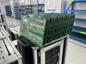
Fournisseur de PCB en cuivre épais
South-Electronic
Choisissez South-Electronic pour une qualité inégalée, une fiabilité et une valeur exceptionnelle pour vos besoins en PCB. Faites l'expérience de la différence avec notre service complet de PCB en cuivre épais – de la conception initiale à l'assemblage final, nous assurons la précision, la durabilité et le respect des normes industrielles les plus élevées.
Votre fournisseur de confiance de PCB en cuivre épais
Bienvenue chez South-Electronic, où vous découvrirez des PCB en cuivre épais de première qualité, réputés pour leur excellente conductivité et gestion thermique.
Faites confiance à South-Electronic pour une qualité exceptionnelle et une cohérence dans vos projets électroniques. Nos PCB en cuivre épais améliorent la fonctionnalité de vos appareils avec une conductivité électrique supérieure et une dissipation thermique efficace. Collaborez avec nous pour l’excellence et l’innovation dans votre domaine.
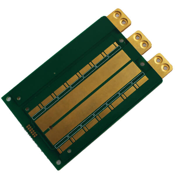
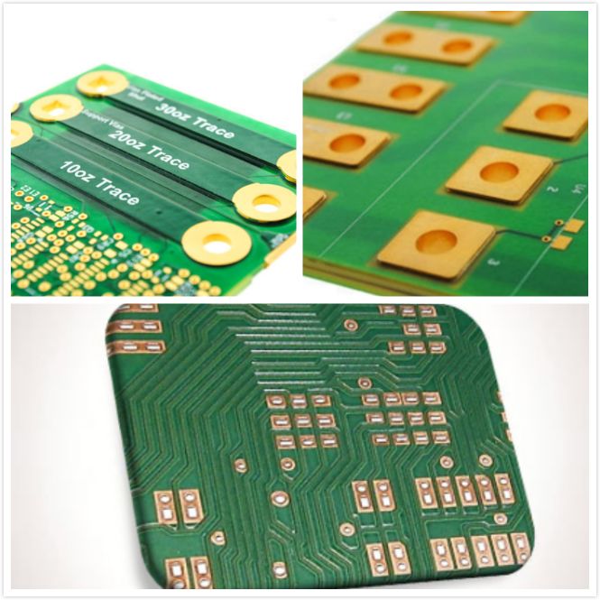
PCB en cuivre épais standard
Il a une épaisseur de cuivre de 2 oz/ft² à 3 oz/ft², ce qui signifie qu'il offre la performance et la conductivité nécessaires pour faire le travail correctement.
PCB en cuivre épais
Il a une épaisseur de cuivre de 4 oz/ft² à 20 oz/ft², ce qui signifie qu'il est conçu pour des environnements à haute puissance comme le contrôle industriel et les systèmes de puissance. Il a la capacité de courant et la gestion de la chaleur nécessaires pour que tout fonctionne sans à-coups.

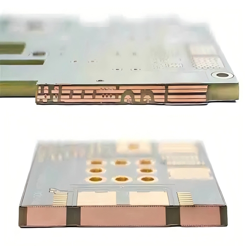
PCB en cuivre extrêmement épais
Il a une épaisseur de cuivre de plus de 20 oz/ft², ce qui signifie qu'il est destiné aux applications extrêmes comme la distribution de haute puissance et la gestion thermique.
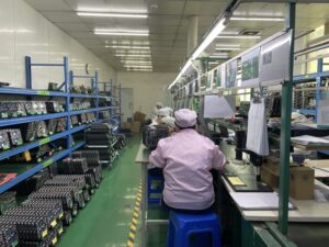
Pourquoi choisir South-Electronic ?
Choisissez South-Electronic. Ils s’y connaissent en PCB en cuivre épais. Ils le fabriqueront exactement comme vous le souhaitez. Profitez d’un service sur mesure, d’une livraison rapide et d’une satisfaction garantie à chaque commande.
-
Flexibilité dans la commande
Votre commande, personnalisée juste pour vous.
Nous pouvons gérer n'importe quelle taille de commande, d'un PCB unique à un grand lot. Vous obtenez exactement ce dont vous avez besoin, fabriqué selon les spécifications de votre projet. Aucune commande n'est trop petite, et nous prêtons attention à chaque détail. -
Équipe expérimentée
Vous profitez de notre décennie d'expertise dans l'industrie.
Bénéficiez de plus d'une décennie d'expertise industrielle avec une équipe aussi expérimentée que dévouée. Nous sommes ici pour vous aider à surmonter avec facilité tous les défis liés aux PCB. -
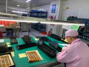
Service complet
Vous obtenez une satisfaction complète avec notre vaste gamme d'équipements.
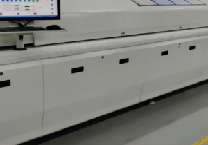
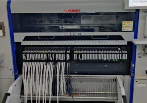
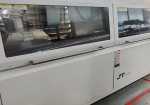
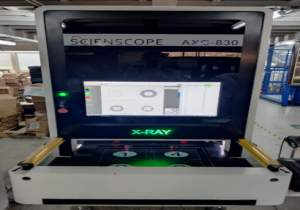
Nous avons une large gamme de capacités de traitement de PCB. De la conception à la livraison, nous disposons de l'équipement et des processus pour garantir que votre commande est réalisée correctement. -
Livraison rapide
Vous profitez de nos délais de production rapides et efficaces.
Nous travaillons rapidement pour vous livrer vos PCB à temps, à chaque fois. -
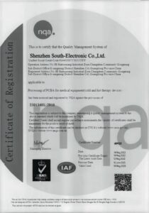
Satisfaction garantie
Vous êtes assuré de la qualité et de la communication claire avec notre certification ISO9001.
Votre satisfaction est notre priorité, et nous nous engageons à dépasser vos attentes avec chaque commande.
Projet lié que nous avons réalisé
Avis des clients
Questions courantes
Questions les plus populaires
Envoyez-nous un message
Plus vous remplissez de détails, plus nous pourrons avancer rapidement à l’étape suivante.


Le guide complet pour PCB en cuivre épais
Contenu
Chapitre 1
Introduction aux PCB en cuivre épais
Les PCB en cuivre épais sont des circuits imprimés avec des couches de cuivre beaucoup plus épaisses que les PCB standards. Les couches de cuivre sur les PCB en cuivre épais peuvent aller de 105 µm (3 oz/ft²) à 400 µm (12 oz/ft²) ou plus. Ces PCB sont conçus pour gérer des courants élevés, supporter des températures élevées et offrir une meilleure résistance mécanique. Les PCB en cuivre épais sont utilisés lorsque les PCB standards échouent en raison de la surchauffe, d’une capacité de courant insuffisante ou de l’usure.
Le cuivre plus épais aide la carte à conduire l’électricité et à dissiper la chaleur de manière plus efficace, ce qui est important dans les applications électroniques à haute puissance telles que les systèmes d’alimentation, l’électronique automobile et la machinerie industrielle. Les PCB en cuivre épais sont également importants dans les applications où la carte doit bien fonctionner dans des conditions difficiles, comme les systèmes d’énergie renouvelable et l’électronique militaire.
Les PCB en cuivre épais sont importants dans l’électronique moderne. Ils offrent de meilleures performances et durent plus longtemps, surtout dans les environnements où les dispositifs sont exposés à des températures élevées, des courants élevés ou des secousses constantes. Cela rend les PCB en cuivre épais essentiels dans les industries qui nécessitent des cartes durables et performantes, comme les télécommunications, l’aérospatiale et la fabrication de véhicules électriques.
Chapitre 2
Types courants de PCB en cuivre épais
Les PCB en cuivre épais sont très recherchés dans des industries telles que l’automobile, l’électronique de puissance, les télécommunications et les machines industrielles car ils offrent plusieurs avantages distincts. Ces plaques sont conçues pour gérer des charges de puissance plus élevées, améliorer la dissipation thermique et offrir une plus grande durabilité par rapport aux PCB standard. Voici quelques-uns des avantages clés :
- Excellente Dissipation de la Chaleur
Les PCB en cuivre épais sont capables de dissiper la chaleur plus efficacement que les PCB standard. Les couches de cuivre plus épaisses offrent une plus grande surface pour le transfert de chaleur, permettant à la plaque de supporter des charges thermiques plus élevées sans surchauffe. Cela est particulièrement important dans des applications telles que les alimentations électriques et les chargeurs de véhicules électriques, où une chaleur excessive peut endommager les composants et réduire la durée de vie du dispositif. En utilisant des PCB en cuivre épais, les fabricants peuvent garantir des performances stables dans des environnements à haute température, améliorant ainsi la fiabilité globale de leurs produits.
- Durabilité Améliorée
Les PCB en cuivre épais sont beaucoup plus robustes que les PCB standard. Les couches de cuivre plus épaisses offrent une résistance mécanique supplémentaire, rendant la plaque plus résistante aux stress thermiques et physiques. Cette durabilité est particulièrement importante dans les environnements où le PCB peut être soumis à des conditions difficiles telles que des vibrations, des chocs ou des températures extrêmes. Par exemple, les PCB en cuivre épais sont couramment utilisés dans les équipements industriels et les électroniques de qualité militaire, où la fiabilité et la longévité sont cruciales. Ils peuvent supporter des cycles thermiques répétés sans développer de fissures ou d’autres formes de dommages, garantissant une durée de vie opérationnelle plus longue.
- Capacité à Transporter des Courants Plus Élevés
Les PCB en cuivre épais peuvent transporter des courants considérablement plus élevés par rapport aux PCB standard. Les couches de cuivre plus épaisses permettent des traces plus larges et plus épaisses, capables de transporter plus de courant sans générer de chaleur excessive. Cela rend les PCB en cuivre épais idéaux pour des applications à haute puissance telles que les amplificateurs de puissance, les convertisseurs à courant élevé et les moteurs électriques. En revanche, les PCB standard avec des couches de cuivre plus minces auraient du mal à gérer ces charges de courant élevées, entraînant un potentiel d’échec dû à la surchauffe ou à la combustion des conducteurs.
- Conception Compacte avec Haute Performance
Les PCB en cuivre épais permettent aux concepteurs d’atteindre une performance plus élevée dans un espace plus compact. En intégrant des couches de cuivre plus épaisses, les fabricants peuvent réduire le nombre de composants ou simplifier le circuit tout en maintenant une gestion thermique et de puissance élevée. Cela est particulièrement utile dans les applications où l’espace est limité, telles que l’électronique automobile ou les dispositifs médicaux, où il est crucial de maximiser la performance tout en minimisant la taille.
- Fiabilité dans des Conditions Extrêmes
Les PCB en cuivre épais sont conçus pour bien fonctionner dans des conditions environnementales extrêmes, telles que l’humidité élevée, les environnements corrosifs ou les opérations à haute altitude. Cela en fait un excellent choix pour les applications aérospatiales et de défense, où l’électronique est exposée à des éléments difficiles. Ces plaques peuvent fonctionner de manière fiable dans une large gamme de températures et résister à la dégradation avec le temps, garantissant une performance et une stabilité à long terme.
Comparaison avec les PCB Standard
Alors que les PCB standard sont suffisants pour des applications à faible puissance et à usage général, ils sont insuffisants dans des scénarios à haute puissance et haute performance. Les PCB standard ont généralement des couches de cuivre allant de 1 oz/ft² à 3 oz/ft², limitant leur capacité à transporter du courant et leur performance thermique. En revanche, les PCB en cuivre épais peuvent gérer des courants beaucoup plus élevés et dissiper la chaleur plus efficacement, ce qui en fait une option bien meilleure pour les applications nécessitant une puissance et une fiabilité strictes.
De plus, les PCB standard sont plus susceptibles d’être endommagés par des cycles thermiques, des stress mécaniques et une exposition à des environnements extrêmes. Les PCB en cuivre épais, avec leur durabilité et leur résistance mécanique améliorées, fournissent une solution plus fiable pour les applications critiques où les arrêts ou les échecs ne sont pas une option.
En résumé, les PCB en cuivre épais offrent des avantages significatifs en termes de dissipation de la chaleur, de durabilité, de capacité de courant et de fiabilité, ce qui en fait un choix idéal pour les applications à haute puissance nécessitant une performance supérieure et une longévité.
Chapitre 3
Considérations de conception pour les PCB en cuivre épais
Les PCB en cuivre épais sont très recherchés dans des industries telles que l’automobile, l’électronique de puissance, les télécommunications et les machines industrielles, car ils offrent plusieurs avantages distincts. Ces plaques sont conçues pour gérer des charges de puissance plus élevées, améliorer la dissipation thermique et offrir une plus grande durabilité par rapport aux PCB standard. Voici quelques-uns des avantages clés :
- Excellente Dissipation de la Chaleur
Les PCB en cuivre épais sont capables de dissiper la chaleur plus efficacement que les PCB standard. Les couches de cuivre plus épaisses offrent une plus grande surface pour le transfert de chaleur, permettant à la plaque de supporter des charges thermiques plus élevées sans surchauffe. Cela est particulièrement important dans des applications telles que les alimentations électriques et les chargeurs de véhicules électriques, où une chaleur excessive peut endommager les composants et réduire la durée de vie de l’appareil. En utilisant des PCB en cuivre épais, les fabricants peuvent garantir des performances stables dans des environnements à haute température, améliorant ainsi la fiabilité globale de leurs produits.
- Durabilité Améliorée
Les PCB en cuivre épais sont beaucoup plus robustes que les PCB standard. Les couches de cuivre plus épaisses offrent une résistance mécanique supplémentaire, rendant la plaque plus résistante aux stress thermiques et physiques. Cette durabilité est particulièrement importante dans les environnements où le PCB peut être soumis à des conditions difficiles telles que des vibrations, des chocs ou des températures extrêmes. Par exemple, les PCB en cuivre épais sont couramment utilisés dans les équipements industriels et les électroniques de qualité militaire, où la fiabilité et la longévité sont cruciales. Ils peuvent supporter des cycles thermiques répétés sans développer de fissures ou d’autres formes de dommages, garantissant une durée de vie opérationnelle plus longue.
- Capacité à Transporter des Courants Plus Élevés
Les PCB en cuivre épais peuvent transporter des courants significativement plus élevés par rapport aux PCB standard. Les couches de cuivre plus épaisses permettent des traces plus larges et plus épaisses, pouvant transporter plus de courant sans générer de chaleur excessive. Cela rend les PCB en cuivre épais idéaux pour des applications à haute puissance telles que les amplificateurs de puissance, les convertisseurs à courant élevé et les moteurs électriques. En revanche, les PCB standard avec des couches de cuivre plus fines auraient du mal à gérer ces charges de courant élevées, entraînant un potentiel de défaillance dû à la surchauffe ou à la combustion des conducteurs.
- Conception Compacte avec Haute Performance
Les PCB en cuivre épais permettent aux concepteurs d’atteindre des performances plus élevées dans un espace plus compact. En intégrant des couches de cuivre plus épaisses, les fabricants peuvent réduire le nombre de composants ou simplifier le circuit tout en maintenant une gestion thermique et de puissance élevées. Cela est particulièrement utile dans des applications où l’espace est limité, telles que l’électronique automobile ou les dispositifs médicaux, où il est crucial de maximiser les performances tout en minimisant la taille.
- Fiabilité dans des Conditions Extrêmes
Les PCB en cuivre épais sont conçus pour bien fonctionner dans des conditions environnementales extrêmes, telles que l’humidité élevée, les environnements corrosifs ou les opérations à haute altitude. Cela en fait un excellent choix pour les applications aérospatiales et de défense, où l’électronique est exposée à des éléments difficiles. Ces plaques peuvent fonctionner de manière fiable dans une large gamme de températures et résister à la dégradation au fil du temps, garantissant des performances et une stabilité à long terme.
Comparaison avec les PCB Standard
Alors que les PCB standard sont suffisants pour des applications à faible puissance et à usage général, ils sont insuffisants dans des scénarios à haute puissance et haute performance. Les PCB standard ont généralement des couches de cuivre allant de 1 oz/ft² à 3 oz/ft², ce qui limite leur capacité à transporter du courant et leur performance thermique. En revanche, les PCB en cuivre épais peuvent gérer des courants beaucoup plus élevés et dissiper la chaleur plus efficacement, ce qui en fait une option bien meilleure pour des applications nécessitant des exigences strictes en matière de puissance et de fiabilité.
De plus, les PCB standard sont plus susceptibles de subir des dommages dus à des cycles thermiques, à un stress mécanique et à une exposition à des environnements extrêmes. Les PCB en cuivre épais, avec leur durabilité améliorée et leur résistance mécanique, offrent une solution plus fiable pour des applications critiques où les temps d’arrêt ou les défaillances ne sont pas une option.
En résumé, les PCB en cuivre épais offrent des avantages significatifs en termes de dissipation thermique, de durabilité, de capacité de courant et de fiabilité, ce qui en fait un choix idéal pour des applications à haute puissance exigeant des performances supérieures et une longévité.
Chapitre 4
Applications des PCB en cuivre épais
Les PCB en cuivre épais sont utilisés dans des industries qui nécessitent une gestion de haute puissance, une dissipation de chaleur améliorée et une durabilité accrue. Ils sont essentiels dans divers secteurs, notamment l’automobile, l’électronique de puissance, l’équipement industriel, et plus encore. Voici quelques industries spécifiques et applications où les PCB en cuivre épais sont critiques.
- Automobile
Les PCB en cuivre épais sont cruciaux dans l’industrie automobile, en particulier pour les véhicules électriques (VE) et les véhicules hybrides. Ils sont utilisés dans divers composants, notamment :
- Systèmes de contrôle de groupe motopropulseur : Les PCB en cuivre épais gèrent efficacement la puissance dans les moteurs électriques et les unités de contrôle.
- Systèmes de gestion de batterie (BMS) : Les PCB en cuivre épais peuvent supporter des courants élevés et gérer les charges thermiques, ce qui les rend idéaux pour les BMS dans les VE.
- Systèmes d’éclairage LED : Les PCB en cuivre épais dissipent la chaleur, garantissant la longévité et les performances des systèmes LED automobiles.
- Stations de charge : Les PCB en cuivre épais gèrent des courants élevés dans les systèmes de charge des VE, offrant une charge rapide et fiable sans surchauffe.
- Électronique de puissance
Les PCB en cuivre épais sont essentiels dans l’électronique de puissance, où une gestion de haute puissance et une gestion thermique efficace sont nécessaires. Ils sont utilisés dans des applications telles que :
- Alimentation et convertisseurs : Les PCB en cuivre épais sont couramment utilisés dans les unités d’alimentation (PSUs), les onduleurs, et les convertisseurs DC-DC en raison de leur capacité à gérer de lourdes charges de courant et à dissiper la chaleur efficacement.
- Systèmes d’énergie renouvelable : Les PCB en cuivre épais aident à gérer les grandes quantités de courant générées dans les onduleurs solaires et les convertisseurs d’énergie éolienne, assurant une distribution efficace de l’énergie.
- Alimentation électrique sans interruption (UPS) : Les PCB en cuivre épais gèrent des courants élevés pendant les opérations de sauvegarde d’énergie, maintenant la stabilité et la fiabilité.
- Équipement industriel
Les PCB en cuivre épais sont utilisés dans les machines industrielles pour répondre aux exigences de contrôle de puissance, de durabilité et de fonctionnement fiable dans des conditions extrêmes. Quelques applications spécifiques incluent :
- Contrôleurs de moteurs lourds : Les moteurs industriels nécessitent des PCB en cuivre épais pour contrôler les flux de courant importants et éviter la surchauffe pendant le fonctionnement.
- Systèmes de distribution de puissance : Les PCB en cuivre épais sont utilisés dans les tableaux de distribution électrique dans les environnements industriels pour gérer les courants élevés de manière sécurisée et fiable.
- Robotique et automatisation : Les PCB en cuivre épais gèrent la puissance requise pour des opérations complexes et de haute performance dans les robots industriels.
- Télécommunications
Les PCB en cuivre épais sont bénéfiques dans les applications de télécommunications qui nécessitent une puissance élevée et une fiabilité, telles que :
- Tours de téléphonie mobile et stations de base : Les PCB en cuivre épais gèrent la puissance nécessaire pour transmettre des signaux sur de longues distances, garantissant des performances constantes et minimisant la perte d’énergie.
- Dispositifs de transmission à haute fréquence : Les PCB en cuivre épais maintiennent l’intégrité du signal et gèrent de lourdes charges de puissance dans les équipements de télécommunications transmettant de grandes quantités de données sur des distances significatives.
- Aérospatiale et défense
Les PCB en cuivre épais sont utilisés dans les applications aérospatiales et militaires parce qu’ils peuvent résister à des environnements difficiles et fonctionner de manière fiable dans des conditions extrêmes :
- Systèmes avioniques : Les PCB en cuivre épais sont utilisés dans les systèmes de contrôle et de navigation des avions, où la fiabilité et la gestion thermique sont cruciales.
- Alimentation électrique de qualité militaire : Les PCB en cuivre épais gèrent des courants élevés et supportent des températures extrêmes et des vibrations mécaniques dans les alimentations militaires.
- Systèmes de communication par satellite : Les PCB en cuivre épais sont utilisés pour la distribution de puissance et le contrôle de communication dans les satellites, où la durabilité et l’efficacité sont essentielles.
- Énergie renouvelable
Les PCB en cuivre épais sont vitaux dans le secteur de l’énergie renouvelable, où les systèmes nécessitent de convertir et de distribuer de niveaux élevés de puissance efficacement :
- Onduleurs solaires : Les PCB en cuivre épais gèrent les lourdes charges de courant générées par les panneaux solaires, assurant une conversion et une distribution efficace de l’énergie.
- Contrôleurs d’éoliennes : Les PCB en cuivre épais sont idéaux pour les contrôleurs des systèmes d’énergie éolienne, où la stabilité et la durabilité sont cruciales.
- Dispositifs médicaux
Les PCB en cuivre épais sont utilisés dans des dispositifs médicaux haute puissance qui nécessitent une livraison stable de la puissance, tels que :
- Systèmes d’imagerie : Les PCB en cuivre épais gèrent des courants de haute puissance dans des appareils comme les machines à rayons X, les scanners IRM, et les scanners CT, garantissant une imagerie fiable.
- Systèmes de surveillance des patients : Les PCB en cuivre épais distribuent l’énergie efficacement, assurant un fonctionnement ininterrompu pour la sécurité des patients.
Conclusion
Les PCB en cuivre épais sont essentiels dans les applications haute puissance et haute performance à travers de multiples industries. Ils sont critiques pour les véhicules électriques, les alimentations électriques, l’équipement industriel, les télécommunications, l’aérospatiale et la défense, l’énergie renouvelable et les dispositifs médicaux. La capacité des PCB en cuivre épais à gérer des courants élevés, à dissiper la chaleur et à résister à des conditions extrêmes les rend le choix privilégié pour des applications qui nécessitent performance et fiabilité.

Chapitre 5
Avantages de l'utilisation des PCB en cuivre épais
Les PCB en cuivre épais sont la meilleure option lorsque vous avez besoin d’une carte haute performance et haute puissance pour diverses industries. Ils offrent des avantages qui vont au-delà de ce que vous obtenez avec les PCB standard, et ils sont le choix idéal pour les industries où la dissipation thermique, la capacité de transport de courant et la durabilité sont critiques. Voici quelques-uns des avantages de l’utilisation des PCB en cuivre épais :
- Ils dissipent mieux la chaleur.
Un des grands avantages des PCB en cuivre épais est qu’ils sont excellents pour dissipar la chaleur. Avec des couches de cuivre plus épaisses, la chaleur générée par des composants à courant élevé peut se répandre plus efficacement à travers la carte. Cela rend les PCB en cuivre épais parfaits pour les alimentations électriques, l’éclairage LED et l’électronique automobile, où la surchauffe peut nuire aux performances et à la durée de vie. En gérant bien la chaleur, ces PCB aident à prévenir les pannes de composants et à assurer un fonctionnement fluide, même lorsque vous tirez beaucoup de puissance.
- Ils sont plus durables.
Les PCB en cuivre épais sont naturellement plus durables que les PCB standard en raison de leurs couches de cuivre plus épaisses. Cette épaisseur supplémentaire rend la carte plus résistante au stress thermique, à l’usure mécanique et aux facteurs environnementaux. Dans des industries telles que l’automobile, l’aérospatiale et l’équipement industriel, où les dispositifs doivent faire face à des températures extrêmes, à des vibrations et à un stress mécanique, les PCB en cuivre épais dureront plus longtemps et performeront mieux. Les PCB standard avec des couches de cuivre plus fines ont tendance à se détériorer dans ces environnements difficiles.
- Ils peuvent supporter plus de courant.
Un autre grand avantage des PCB en cuivre épais est qu’ils peuvent gérer des courants plus élevés. Les traces de cuivre plus épaisses peuvent supporter des charges plus importantes sans surchauffe, ce qui est essentiel dans des applications telles que l’électronique de puissance, les systèmes de recharge de véhicules électriques et les contrôleurs de moteurs haute puissance. Les PCB standard avec des couches de cuivre plus fines auraient des difficultés à gérer ces courants élevés, entraînant surchauffe et défaillance du circuit. En utilisant des PCB en cuivre épais, vous pouvez concevoir des systèmes avec des densités de puissance plus élevées tout en restant sûrs et efficaces.
- Ils vous permettent de concevoir des systèmes plus petits et plus denses.
Les PCB en cuivre épais vous permettent de concevoir des dispositifs plus petits tout en gérant de lourdes charges de puissance. Avec ces PCB, vous pouvez réduire la taille de vos appareils sans sacrifier les performances. Cela est particulièrement important dans des applications telles que l’électronique grand public, les dispositifs médicaux et les équipements de télécommunications, où vous avez besoin d’une haute densité de puissance dans un espace réduit. Les PCB standard pourraient nécessiter des conceptions plus grandes ou plus complexes pour gérer la même puissance, donc les PCB en cuivre épais sont plus efficaces.
- Ils sont plus fiables dans des environnements difficiles.
Dans les industries où les composants électroniques doivent faire face à des environnements difficiles—comme une humidité élevée, des températures extrêmes, ou un stress mécanique—les PCB en cuivre épais sont plus fiables. Ils sont moins susceptibles de faillir en raison de la corrosion, de l’oxydation ou de dommages physiques, ce qui les rend parfaits pour des applications aérospatiales, militaires et d’automatisation industrielle. Ils sont conçus pour supporter des conditions difficiles et continuer à bien performer pendant longtemps.
Comment les PCB en cuivre épais se comparent aux PCB standard
Les PCB standard sont adéquats pour des applications à faible puissance et moins exigeantes, mais ils ne suffisent pas lorsque vous avez besoin de haute puissance et de haute performance. La principale différence entre les PCB standard et les PCB en cuivre épais est l’épaisseur des couches de cuivre. Les PCB standard ont généralement des couches de cuivre entre 1 oz/ft² et 3 oz/ft², tandis que les PCB en cuivre épais peuvent avoir des couches de cuivre de 4 oz/ft² à 12 oz/ft² ou plus.
Les principales différences entre les PCB en cuivre épais et les PCB standard :
- Capacité de courant : Les PCB en cuivre épais peuvent gérer beaucoup plus de courant que les PCB standard. Cela en fait le meilleur choix pour les applications gourmandes en énergie, tandis que les PCB standard pourraient surchauffer et échouer dans les mêmes conditions.
- Dissipation de chaleur : Les PCB en cuivre épais excellent dans l’élimination de la chaleur car ils contiennent plus de cuivre. Les PCB standard avec des couches de cuivre plus fines ont du mal à gérer la chaleur, surtout dans les applications à haute puissance.
- Durabilité : Les PCB en cuivre épais sont beaucoup plus durables et meilleurs pour gérer les stress environnementaux, donc ils sont parfaits pour des conditions difficiles. Les PCB standard conviennent aux applications moins exigeantes, mais ils sont plus susceptibles d’échouer dans des environnements extrêmes.
- Efficacité de taille : Les PCB en cuivre épais peuvent supporter une puissance élevée dans un design compact, donc ils sont excellents pour des applications nécessitant une petite empreinte mais une grande performance. Les PCB standard pourraient nécessiter des conceptions plus grandes ou plus de composants pour réaliser la même puissance.
Conclusion
Les PCB en cuivre épais représentent une excellente solution lorsque vous avez besoin de haute puissance, d’une excellente gestion thermique et de durabilité dans des environnements difficiles. Que vous conceviez pour l’électronique automobile, les alimentations électriques ou l’équipement industriel, les PCB en cuivre épais vous offrent fiabilité, efficacité et performance à long terme.
Chapitre 6
Comment choisir l'épaisseur de cuivre appropriée pour votre projet ?
Lorsque vous choisissez l’épaisseur de cuivre appropriée pour votre projet de PCB, il s’agit avant tout de performance, de durabilité et de sécurité. L’épaisseur de la couche de cuivre affecte la quantité de courant que la carte peut supporter, son efficacité à dissiper la chaleur et sa fiabilité. Pour choisir la bonne épaisseur de cuivre, vous devez réfléchir aux besoins de votre application en termes de gestion de l’énergie, de gestion thermique et de l’environnement dans lequel elle se trouvera. Voici un guide pour vous aider à choisir la bonne épaisseur de cuivre pour votre projet.
- Comprendre comment l’épaisseur de cuivre est mesurée
L’épaisseur de cuivre dans les PCB est mesurée en onces par pied carré (oz/ft²), ce qui vous indique combien de cuivre se trouve sur un pied carré de la surface de la carte. Les épaisseurs de cuivre standard sont :
- 1 oz/ft² = 35 micromètres (µm)
- 2 oz/ft² = 70 micromètres (µm)
- 3 oz/ft² = 105 micromètres (µm)
Pour les PCB en cuivre épais, les couches de cuivre peuvent varier de 4 oz/ft² (140 µm) à 12 oz/ft² (400 µm) ou plus, selon la quantité d’énergie et de courant que l’application nécessite.
- Considérer les exigences en matière de puissance
La première chose à faire lorsque vous choisissez la bonne épaisseur de cuivre est de déterminer combien de puissance votre circuit nécessite. Si vous avez beaucoup de puissance qui traverse la carte, vous aurez besoin de couches de cuivre plus épaisses pour gérer le courant sans surchauffer ni endommager le PCB. Par exemple :
- Les applications à faible puissance (comme l’électronique grand public) peuvent utiliser une épaisseur standard de 1 oz ou 2 oz de cuivre.
- Les applications à puissance moyenne (comme les contrôleurs de moteurs ou l’éclairage LED) nécessitent généralement une épaisseur de cuivre de 2 oz à 3 oz pour fonctionner de manière fiable.
- Les applications à haute puissance (comme les alimentations électriques, les chargeurs de véhicules électriques ou les systèmes de contrôle industriels) nécessitent une épaisseur de cuivre de 4 oz ou plus pour gérer les courants élevés en toute sécurité et efficacité.
Plus le cuivre est épais, plus il peut supporter de courant sans surchauffer ou échouer.
- Tenir compte des besoins de gestion thermique
L’épaisseur de cuivre est également importante pour la dissipation de chaleur, surtout lorsque vous avez des courants élevés. Si un courant important passe à travers la carte, il peut générer beaucoup de chaleur. Des couches de cuivre plus épaisses peuvent mieux répartir la chaleur sur le PCB, ce qui réduit le risque de surchauffe et améliore la performance thermique globale du circuit. Cela est particulièrement important pour des applications comme l’électronique de puissance, les systèmes automobiles et les systèmes d’énergie renouvelable, où il est nécessaire de gérer la chaleur pour maintenir la stabilité et la sécurité du système.
Si votre application génère beaucoup de chaleur, comme la conversion d’énergie ou les systèmes de contrôle industriels, vous devriez envisager d’utiliser une épaisseur de cuivre de 4 oz ou plus pour améliorer les performances thermiques et la fiabilité.
- Réfléchir à la taille et à la complexité de la conception du PCB
Des couches de cuivre plus épaisses vous permettent de créer des conceptions plus compactes, car vous pouvez avoir des traces plus larges et plus épaisses pour transporter des courants élevés sans augmenter la taille de la carte. Si vous avez un projet avec beaucoup de circuits complexes dans un petit espace, comme l’électronique automobile ou les équipements de télécommunications, un cuivre plus épais peut vous aider à obtenir la disposition souhaitée sans sacrifier les performances. Mais souvenez-vous qu’à mesure que l’épaisseur du cuivre augmente, cela peut affecter la facilité de fabrication et le coût du PCB. Vous devez équilibrer la complexité du design avec l’espace et le budget dont vous disposez.
- Tenir compte de l’environnement
L’environnement dans lequel votre PCB se trouvera affecte également l’épaisseur de cuivre que vous devriez utiliser. Si votre application sera soumise à des conditions difficiles, comme une humidité élevée, des produits chimiques corrosifs ou des températures extrêmes, un cuivre plus épais peut aider la carte à résister à ces facteurs. Les industries comme l’aérospatiale, la défense et l’automatisation industrielle utilisent souvent des couches de cuivre plus épaisses car cela rend le PCB plus durable et lui permet de durer plus longtemps.
- Suivre les normes et directives de l’industrie
Certaines industries ont des normes et des directives qui stipulent l’épaisseur de cuivre nécessaire. Par exemple, dans l’électronique de puissance, il peut y avoir des règles qui exigent que vous ayez une épaisseur de cuivre minimum pour être en sécurité et respecter les normes de l’industrie. Vous devriez examiner ces directives lors de la conception de votre PCB pour vous assurer qu’il répond aux spécifications appropriées pour votre secteur.
- Parler à votre fabricant de PCB
Une fois que vous connaissez les besoins de votre projet en matière d’énergie, de thermique, de conception et d’environnement, il est conseillé de discuter avec votre fabricant de PCB pour vous assurer que l’épaisseur de cuivre souhaitée sera fonctionnelle. Ils peuvent vous informer sur la facilité ou la difficulté de fabrication du PCB avec des couches de cuivre plus épaisses et sur le coût que cela engendre. Ils peuvent également vous conseiller sur les meilleures pratiques de conception pour garantir que votre PCB fonctionne comme vous le souhaitez.
Conclusion
Choisir la bonne épaisseur de cuivre consiste à équilibrer les exigences énergétiques, la gestion de la chaleur, la complexité de la conception et l’environnement. Les couches de cuivre plus épaisses sont importantes lorsque vous devez transporter beaucoup de courant et avoir de bonnes performances thermiques. Cependant, elles coûtent également plus cher et peuvent être plus difficiles à fabriquer. En comprenant les besoins de votre projet et en parlant à votre fabricant de PCB, vous pouvez faire un bon choix qui assurera un excellent fonctionnement de votre PCB dans votre application.

Chapitre 7
Facteurs de coût pour les PCB en cuivre épais
Le coût de fabrication des PCB en cuivre épais peut varier considérablement en fonction de plusieurs facteurs, notamment l’épaisseur du cuivre, la complexité de la conception et le volume de production. Comprendre ces facteurs peut vous aider à prendre des décisions éclairées pour équilibrer performance et coût, en vous assurant d’obtenir la meilleure valeur pour votre projet PCB. Voici un aperçu des principaux facteurs de coût et des conseils pour optimiser votre conception afin de minimiser les dépenses sans compromettre la qualité.
- Épaisseur du cuivre
Le principal facteur de coût pour les PCB en cuivre épais est l’épaisseur de la couche de cuivre elle-même. Plus le cuivre est épais, plus il faut de matériau, ce qui entraîne des coûts de matériaux plus élevés. Par exemple :
- Les PCB standard avec 1 oz/ft² de cuivre sont moins chers car ils utilisent moins de cuivre.
- Les PCB en cuivre épais avec 4 oz/ft² ou plus augmentent considérablement les coûts de matériau en raison du cuivre supplémentaire nécessaire.
De plus, le processus de fabrication des PCB en cuivre épais est plus complexe, nécessitant des étapes supplémentaires telles que le gravage et le plaquage améliorés pour gérer le cuivre plus épais. Cela contribue également à des coûts de production plus élevés. Le choix de l’épaisseur du cuivre doit être aligné avec les exigences de courant et thermiques de l’application pour éviter des dépenses inutiles.
- Complexité de la conception
La complexité de la conception est un autre facteur de coût majeur dans la production de PCB en cuivre épais. Les conceptions complexes avec un routage détaillé, plusieurs couches ou des composants à pas fin nécessitent plus de temps et de ressources pour la fabrication. Certains aspects clés qui peuvent augmenter les coûts comprennent :
- PCBs multicouches : Bien qu’un PCB en cuivre épais à une seule couche soit moins cher à produire, des cartes multicouches sont nécessaires pour des applications plus complexes, et le nombre de couches impacte directement le prix.
- Composants à pas fin : Les PCB avec des composants très petits et un espacement serré nécessitent des processus de fabrication plus précis, augmentant les coûts de main-d’œuvre et d’équipement.
- Vias et plaquage : Les conceptions qui nécessitent plusieurs types de vias (comme des vias aveugles, enfouis ou microvias) ajoutent également à la complexité et au coût de production.
Pour réduire les coûts, il est essentiel de simplifier la conception lorsque cela est possible, en minimisant le nombre de couches ou les fonctionnalités non essentielles qui n’apportent pas de valeur au produit final.
- Volume de production
Le volume de production joue un rôle crucial dans la détermination du coût par unité des PCB en cuivre épais. Comme pour la plupart des processus de fabrication, les grandes séries de production tendent à entraîner des coûts par unité plus bas en raison des économies d’échelle. Les fabricants de PCB offrent souvent des réductions pour les commandes en gros car ils peuvent répartir les coûts d’installation et de production sur un plus grand nombre d’unités.
Pour des volumes de production plus petits, comme des prototypes ou des petites séries, le coût par unité est significativement plus élevé car les coûts d’installation restent constants, peu importe le nombre de cartes produites. Si possible, le regroupement des commandes ou la planification pour des volumes de production plus importants peut aider à réduire les coûts.
- Matériaux spécialisés
Dans certaines applications, des matériaux spécialisés peuvent être nécessaires pour compléter les couches de cuivre plus épaisses, tels que des substrats haute température ou des matériaux d’isolation avancés. Ces matériaux peuvent augmenter le coût global du PCB. Par exemple, des substrats comme le FR4 peuvent suffire pour des applications standards, mais des matériaux haute température comme le polyimide ou la céramique peuvent être nécessaires pour des environnements plus exigeants, ce qui augmente encore le coût.
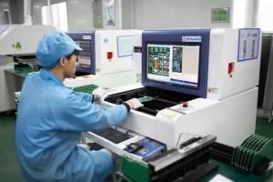
- Processus de fabrication
La complexité du processus de fabrication influence également le coût. Les couches de cuivre plus épaisses nécessitent des processus de gravure et de plaquage plus précis, ce qui peut impliquer des temps de traitement plus longs et des équipements plus avancés. De plus, certains fabricants peuvent utiliser des techniques spécialisées, telles que le laminage séquentiel ou plusieurs cycles de plaquage, pour produire des PCB en cuivre épais de haute qualité. Ces processus avancés contribuent à des coûts de production plus élevés par rapport aux PCB standard.
Conseils pour optimiser la conception pour équilibrer performance et coût
- Ajustez l’épaisseur de votre cuivre
Bien qu’il puisse être tentant d’utiliser le cuivre le plus épais possible pour une durabilité accrue et une capacité de courant, cette approche peut entraîner des augmentations de coût inutiles. Évaluez soigneusement les besoins en puissance et en chaleur de votre application pour sélectionner l’épaisseur de cuivre optimale. Par exemple, si votre conception nécessite seulement 4 oz/ft² de cuivre pour fonctionner de manière fiable, utiliser 6 oz/ft² de cuivre augmenterait les coûts sans fournir d’avantages supplémentaires.
- Simplifiez la disposition du PCB
Dans la mesure du possible, visez à simplifier la disposition de votre PCB. Réduire le nombre de couches, minimiser l’utilisation de types de vias spéciaux et éliminer les fonctionnalités non essentielles peut réduire considérablement les coûts de fabrication. Collaborez avec votre équipe de conception pour identifier les domaines où la conception peut être rationalisée sans sacrifier la fonctionnalité.
- Envisagez des matériaux alternatifs
Si votre application le permet, envisagez d’utiliser des matériaux plus économiques pour le substrat du PCB. Bien que certains matériaux spécialisés puissent être nécessaires pour des environnements extrêmes, des matériaux standards comme le FR4 peuvent suffire pour de nombreuses applications de PCB en cuivre épais. Choisir le bon substrat pour votre projet peut contribuer à réduire les coûts globaux des matériaux.
Cahpter 8
Résolution des problèmes courants avec les PCB en cuivre épais
Bien que les PCB en cuivre épais soient robustes et fiables, ils peuvent rencontrer des problèmes spécifiques qui nécessitent des stratégies efficaces de dépannage et d’entretien. Ci-dessous, nous décrivons les problèmes courants et fournissons des solutions, ainsi que des conseils d’entretien pour prolonger la durée de vie de ces PCB.
Problèmes courants et solutions
Distribution de chaleur inégale :
- Problème : Les PCB en cuivre épais peuvent parfois présenter une distribution de chaleur inégale en raison de leur masse thermique élevée, ce qui peut entraîner des points chauds.
- Solution : Mettre en œuvre des techniques de gestion thermique telles que l’ajout de vias thermiques ou de dissipateurs thermiques directement au-dessus des points chauds. Assurez-vous que la conception thermique est intégrée à la phase de conception du PCB pour répartir la chaleur uniformément sur la carte.
Difficultés de soudage :
- Problème : La masse thermique élevée du cuivre épais peut entraîner des difficultés pour obtenir une soudure correcte, avec un potentiel de joints de soudure froids.
- Solution : Ajuster le processus de soudage en augmentant les températures de préchauffage et en prolongant les temps de trempage. Utiliser des soudures avec un point de fusion plus élevé et s’assurer que la couverture de pâte à souder est adéquate pour les grandes zones de cuivre.
Incohérences dans le gravage :
- Problème : En raison de l’épaisseur accrue, le gravage du cuivre épais peut parfois entraîner des zones sous-gravées ou sur-gravées, ce qui conduit à des chemins de circuit peu fiables.
- Solution : Optimiser le processus de gravage en contrôlant plus précisément la chimie de l’agent de gravage et la température. Des inspections fréquentes pendant la phase de gravage peuvent aider à détecter toute incohérence tôt.
Tensions mécaniques :
- Problème : Le poids et la rigidité des PCB en cuivre épais peuvent les rendre susceptibles de se plier ou de se déformer, surtout dans les conceptions plus grandes.
- Solution : Soutenir adéquatement le PCB lors de sa manipulation et de son installation. Envisagez d’utiliser des matériaux plus rigides pour le substrat ou de renforcer la structure avec des couches de support supplémentaires.
Conseils d’entretien pour prolonger la vie des PCB en cuivre épais
Nettoyage régulier :
- Conseil : Gardez les PCB propres de la poussière et des résidus chimiques, qui peuvent provoquer de la corrosion avec le temps. Utilisez de l’alcool isopropylique et une brosse douce pour nettoyer délicatement les surfaces.
Inspections périodiques :
- Conseil : Effectuez des inspections régulières pour détecter des signes d’usure, des défauts de soudure ou des dommages mécaniques. Une détection précoce des problèmes peut empêcher leur aggravation.
Gestion thermique :
- Conseil : Assurez-vous de l’efficacité continue de tous les systèmes de gestion thermique en place, tels que les ventilateurs ou les dissipateurs de chaleur. Vérifiez et remplacez régulièrement les matériaux d’interface thermique pour maintenir une dissipation de chaleur optimale.
Contrôles environnementaux :
- Conseil : Stockez et faites fonctionner les PCB dans des environnements contrôlant l’humidité et la température. Une humidité excessive et des fluctuations de température peuvent accélérer la dégradation des matériaux du PCB.
Mises à jour du firmware et tests fonctionnels :
- Conseil : Pour les PCB intégrées dans des systèmes de contrôle logiciel, assurez-vous que les mises à jour du firmware sont appliquées régulièrement et que des tests fonctionnels sont effectués pour vérifier que tous les composants fonctionnent correctement.
En comprenant ces problèmes courants et en mettant en œuvre des pratiques d’entretien approfondies, les utilisateurs de PCB en cuivre épais peuvent considérablement améliorer la fiabilité et prolonger la durée de vie de leurs applications électroniques haute puissance. Ces pratiques garantissent non seulement un performance optimale mais contribuent également à des économies de coûts en minimisant le besoin de réparations ou de remplacements fréquents.
Chapitre 9
Assurance qualité dans les PCB en cuivre épais
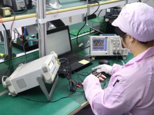
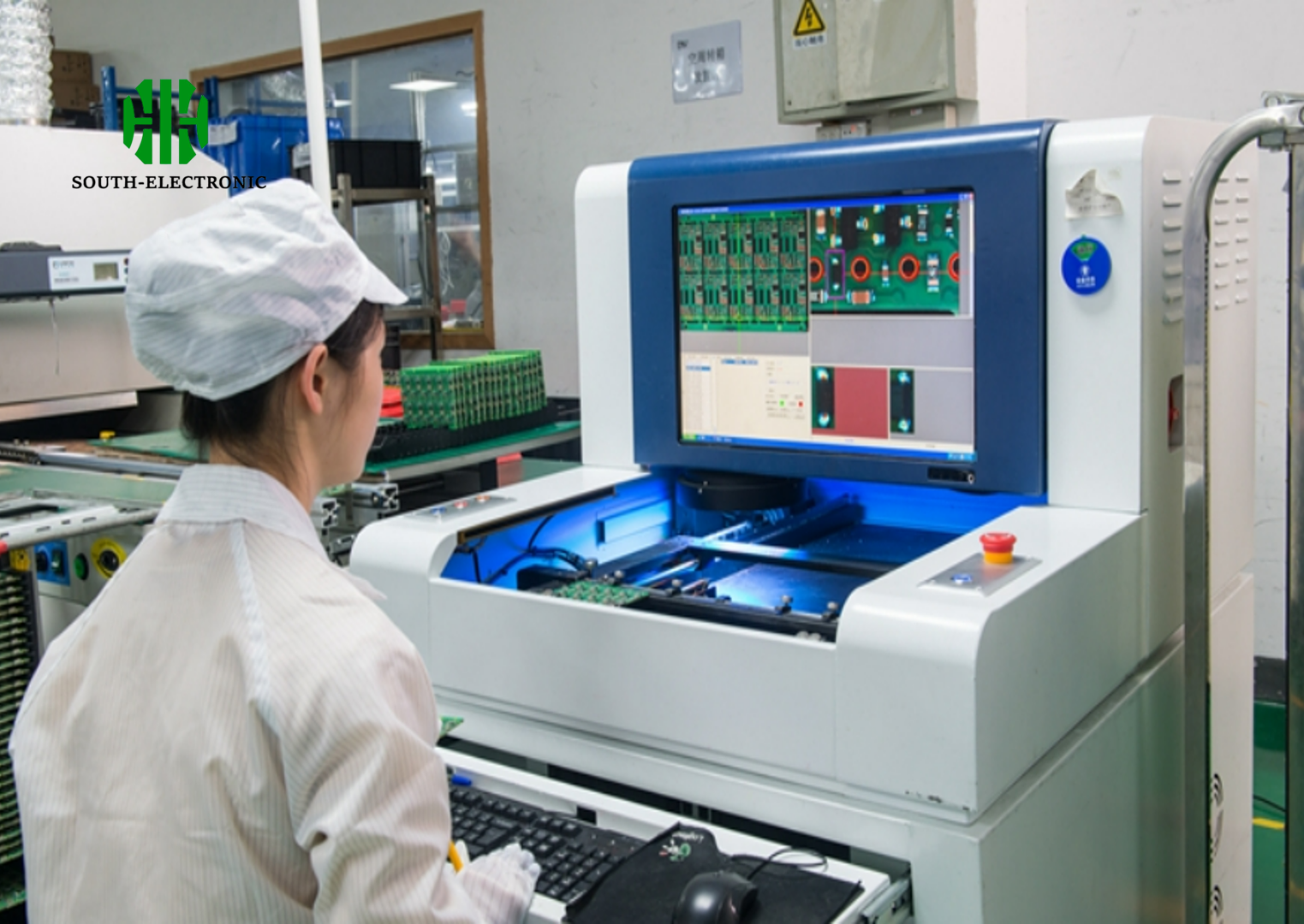
Assurer la qualité des PCB en cuivre épais est crucial pour garantir leur fiabilité et leur performance à long terme dans les applications à haute puissance et à courant élevé. Étant donné les défis uniques associés à la fabrication des PCB en cuivre épais, des tests approfondis et des processus d’assurance qualité sont essentiels. Ces tests garantissent que le PCB répond aux normes électriques, thermiques et mécaniques strictes exigées par des secteurs tels que l’automobile, l’électronique de puissance et l’automatisation industrielle. Ci-dessous, nous présentons quelques méthodes critiques d’assurance qualité utilisées pour les PCB en cuivre épais.
- Test de contrainte thermique
Les PCB en cuivre épais sont souvent utilisés dans des applications à courant élevé où la gestion thermique est critique. Par conséquent, le test de contrainte thermique est une partie fondamentale du processus d’assurance qualité. Ce test évalue la capacité du PCB à résister à des variations extrêmes de température sans délaminage, fissuration ou déformation.
Cycles thermiques : Le PCB est soumis à des cycles répétés de chauffage et de refroidissement pour simuler les conditions difficiles pouvant être rencontrées lors d’une utilisation réelle. Par exemple, dans les environnements automobiles ou industriels, les PCB peuvent subir des variations de température drastiques, il est donc essentiel de s’assurer que la carte peut résister à ces cycles sans dommages.
Intégrité des joints de soudure : Les températures élevées peuvent affecter l’intégrité des joints de soudure. Le test de contrainte thermique garantit que les joints de soudure du PCB restent intacts et qu’il n’y a pas de fissures dans la soudure ou de soulèvement des pads même sous une exposition thermique prolongée.
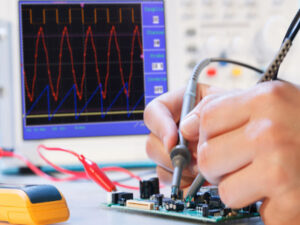
- Validation de la performance électrique
Les PCB en cuivre épais sont conçus pour supporter de forts courants, donc les tests de performance électrique constituent un élément clé du processus d’assurance qualité. Tester les propriétés électriques de la carte garantit qu’elle fonctionne comme prévu sous une charge maximale sans génération excessive de chaleur ou perte de puissance.
Test de continuité : Ce test vérifie la connectivité électrique des traces, garantissant qu’il n’y a pas de coupures ou d’interruptions dans le circuit.
Résistance d’isolation : Tester la résistance d’isolation du PCB garantit qu’il existe un bon isolement entre les différentes traces conductrices et couches. Cela est particulièrement important pour les applications à haute tension où l’isolement est critique pour prévenir les courts-circuits et les défaillances électriques.
Test de courant élevé : Les PCB en cuivre épais doivent être capables de gérer des charges de courant significatives sans provoquer une accumulation excessive de chaleur ou des chutes de tension. Les tests de courant élevé vérifient la capacité du PCB à gérer des conditions de fonctionnement maximales sans surchauffe ou endommagement des composants.
- Test de résistance mécanique
La résistance mécanique est un autre aspect clé de l’assurance qualité pour les PCB en cuivre épais. Ces cartes sont souvent utilisées dans des environnements où elles sont soumises à des contraintes physiques, telles que les vibrations, les chocs ou le pliage.
Test de vibration : Dans des applications comme l’électronique automobile, les PCB sont exposés à des vibrations constantes. Le test de vibration garantit que le PCB et ses composants peuvent résister à ces forces sans craquer ou perdre la connectivité électrique.
Test de pliage : Ce test simule une contrainte mécanique en pliant le PCB pour s’assurer qu’il peut supporter des forces mécaniques sans casser ou endommager les couches ou les composants en cuivre.
- Test de conductivité thermique
Étant donné les couches de cuivre plus épaisses dans ces PCB, le test de conductivité thermique est essentiel pour vérifier que la carte peut dissiper la chaleur efficacement. Une conductivité thermique élevée garantit que le PCB reste froid même sous de lourdes charges électriques.
Test de dissipation thermique : Ce test mesure la capacité du PCB à transférer la chaleur loin des composants critiques et vers des dissipateurs de chaleur ou des matériaux environnants. Assurer une dissipation thermique adéquate aide à prévenir la surchauffe des composants et prolonge la durée de vie du PCB.
Impedance thermique : Tester l’impédance thermique garantit que le PCB peut maintenir des niveaux de température constants sans formation de points chauds. Cela est particulièrement important dans les conceptions multicouches où la chaleur peut s’accumuler entre les couches si elle n’est pas gérée correctement.
- Test de qualité de surface et de soudabilité
La qualité de surface des PCB en cuivre épais est essentielle pour garantir un bon attachement des composants et une performance électrique fiable. Les défauts dans le fini de surface peuvent conduire à une mauvaise soudabilité et affecter la fonctionnalité globale du PCB.
Test de soudabilité : Ce test évalue la qualité d’adhésion de la soudure aux pads en cuivre et aux traces. Une mauvaise soudabilité peut entraîner des connexions faibles ou non fiables, conduisant à des pannes de circuit.
Inspection de surface : L’inspection optique automatisée (AOI) et les inspections visuelles manuelles garantissent que la surface du PCB est exempte de défauts tels que des rayures, des piqûres ou des irrégularités pouvant nuire à la performance ou à la qualité de l’assemblage.
- Test de microsection
Dans les PCB en cuivre épais, la qualité des couches internes et des vias est particulièrement importante, surtout dans les conceptions multicouches. Le test de microsection consiste à couper un échantillon du PCB pour examiner sa structure interne.
Qualité des vias : Le test de microsection aide à identifier des problèmes tels que des vides ou des fissures dans les vias, qui peuvent entraîner une défaillance électrique.
Intégrité des couches internes : Ce test vérifie que les couches de cuivre internes sont correctement formées et exemptes de défauts. Tout problème avec les couches internes pourrait affecter la fiabilité globale et la durée de vie du PCB.
Les PCB en cuivre épais sont utilisés dans des applications exigeantes qui nécessitent une performance fiable sous des charges de courant élevées et des conditions environnementales difficiles. Pour garantir une fiabilité et une efficacité à long terme, il est essentiel de mettre en œuvre des mesures d’assurance qualité complètes, notamment des tests de contrainte thermique, des validations de performance électrique, des tests de résistance mécanique, et plus encore. En collaborant avec un fabricant qui accorde une importance particulière à des tests approfondis, vous pouvez vous assurer que votre PCB en cuivre épais répondra aux normes
Chapitre 10
Assurance qualité dans les PCB en cuivre épais
Assurer la qualité des PCB en cuivre épais est crucial pour garantir leur fiabilité et leur performance à long terme dans les applications à haute puissance et à courant élevé. Étant donné les défis uniques associés à la fabrication des PCB en cuivre épais, des tests approfondis et des processus d’assurance qualité sont essentiels. Ces tests garantissent que le PCB répond aux normes électriques, thermiques et mécaniques strictes exigées par des secteurs tels que l’automobile, l’électronique de puissance et l’automatisation industrielle. Ci-dessous, nous présentons quelques méthodes critiques d’assurance qualité utilisées pour les PCB en cuivre épais.
- Test de contrainte thermique
Les PCB en cuivre épais sont souvent utilisés dans des applications à courant élevé où la gestion thermique est critique. Par conséquent, le test de contrainte thermique est une partie fondamentale du processus d’assurance qualité. Ce test évalue la capacité du PCB à résister à des fluctuations extrêmes de température sans délaminage, fissuration ou déformation.
Cycles thermiques : Le PCB est soumis à des cycles répétés de chauffage et de refroidissement pour simuler les conditions difficiles qu’il pourrait rencontrer lors d’une utilisation réelle. Par exemple, dans des environnements automobiles ou industriels, les PCB peuvent subir des changements de température drastiques, il est donc essentiel de garantir que la carte peut résister à ces cycles sans subir de dommages.
Intégrité des joints de soudure : Des températures élevées peuvent affecter l’intégrité des joints de soudure. Le test de contrainte thermique assure que les joints de soudure du PCB restent intacts et qu’il n’y a pas de fissures dans la soudure ou de soulèvement des pads même sous une exposition thermique prolongée.
- Validation de la performance électrique
Les PCB en cuivre épais sont conçus pour supporter des courants élevés, donc les tests de performance électrique constituent un élément clé du processus d’assurance qualité. Tester les propriétés électriques de la carte garantit qu’elle fonctionne comme prévu sous une charge maximale sans générer de chaleur excessive ou perdre de puissance.
Test de continuité : Ce test vérifie la connectivité électrique des traces, garantissant qu’il n’y a pas de coupures ou d’interruptions dans le circuit.
Résistance d’isolation : Tester la résistance d’isolation du PCB garantit qu’il existe un bon isolement entre les différentes traces conductrices et couches. Cela est particulièrement important pour les applications à haute tension où l’isolement est critique pour prévenir les courts-circuits et les défaillances électriques.
Test de courant élevé : Les PCB en cuivre épais doivent être capables de gérer des charges de courant significatives sans provoquer une accumulation excessive de chaleur ou des baisses de tension. Les tests de courant élevé vérifient la capacité du PCB à gérer des conditions de fonctionnement maximales sans surchauffe ou endommagement des composants.
- Test de résistance mécanique
La résistance mécanique est un autre aspect clé de l’assurance qualité pour les PCB en cuivre épais. Ces cartes sont souvent utilisées dans des environnements où elles sont soumises à des stress physiques, tels que les vibrations, les chocs ou le pliage.
Test de vibration : Dans des applications comme l’électronique automobile, les PCB sont exposés à des vibrations constantes. Le test de vibration garantit que le PCB et ses composants peuvent résister à ces forces sans casser ou perdre la connectivité électrique.
Test de pliage : Ce test simule le stress mécanique en pliant le PCB pour s’assurer qu’il peut supporter des forces mécaniques sans se casser ou endommager les couches en cuivre ou les composants.
- Test de conductivité thermique
Étant donné les couches de cuivre plus épaisses dans ces PCB, le test de conductivité thermique est essentiel pour vérifier que la carte peut dissiper la chaleur efficacement. Une conductivité thermique élevée assure que le PCB reste frais même sous de lourdes charges électriques.
Test de dissipation de chaleur : Ce test mesure la capacité du PCB à transférer la chaleur loin des composants critiques et vers des dissipateurs de chaleur ou des matériaux environnants. Assurer une dissipation de chaleur adéquate aide à prévenir la surchauffe des composants et prolonge la durée de vie du PCB.
Impedance thermique : Tester l’impédance thermique garantit que le PCB peut maintenir des niveaux de température constants sans formation de points chauds. Cela est particulièrement important dans les conceptions multicouches où la chaleur peut s’accumuler entre les couches si elle n’est pas correctement gérée.
- Test de qualité de surface et de soudabilité
La qualité de surface des PCB en cuivre épais est essentielle pour garantir un bon attachement des composants et une performance électrique fiable. Les défauts dans le fini de surface peuvent conduire à une mauvaise soudabilité et affecter la fonctionnalité globale du PCB.
Test de soudabilité : Ce test évalue la qualité d’adhésion de la soudure aux pads en cuivre et aux traces. Une mauvaise soudabilité peut entraîner des connexions faibles ou non fiables, conduisant à des pannes de circuit.
Inspection de surface : L’inspection optique automatisée (AOI) et les inspections visuelles manuelles garantissent que la surface du PCB est exempte de défauts tels que des rayures, des piqûres ou des irrégularités pouvant nuire à la performance ou à la qualité de l’assemblage.
- Test de microsection
Dans les PCB en cuivre épais, la qualité des couches internes et des vias est particulièrement importante, surtout dans les conceptions multicouches. Le test de microsection consiste à couper un échantillon du PCB pour examiner sa structure interne.
Qualité des vias : Le test de microsection aide à identifier des problèmes tels que des vides ou des fissures dans les vias, qui peuvent mener à une défaillance électrique.
Intégrité des couches internes : Ce test vérifie que les couches internes en cuivre sont correctement formées et exemptes de défauts. Tout problème avec les couches internes pourrait affecter la fiabilité globale et la durée de vie du PCB.
Les PCB en cuivre épais sont utilisés dans des applications exigeantes qui nécessitent une performance fiable sous des charges de courant élevées et des conditions environnementales difficiles. Pour garantir une fiabilité et une efficacité à long terme, il est essentiel de mettre en œuvre des mesures d’assurance qualité complètes, y compris des tests de contrainte thermique, des validations de performance électrique, des tests de résistance mécanique, et plus encore.
Contactez-Nous
Où Sommes-Nous ?
Parc Industriel, No. 438 Route Donghuan, No. 438, Shajing Donghuan Road, District Bao'an, Shenzhen, Guangdong, Chine
4ème étage, Bâtiment Zhihui Créatif, No. 2005 Route Xihuan, Shajing, District Baoan, Shenzhen, Chine
CHAMBRE A1-13, ÉTAGE 3, CENTRE INDUSTRIEL YEE LIM, 2-28 RUE KWAI LOK, KWAI CHUNG HK
service@southelectronicpcb.com
Téléphone : +86 400 878 3488
Envoyez-nous un message
Plus vous remplissez de détails, plus nous pourrons avancer rapidement à l’étape suivante.

