
Custom 4-Layer PCB Manufacturing Services
Min trace 3/3 mil | ENIG / HASL | FR-4 & High-TG | AOI & E-Test
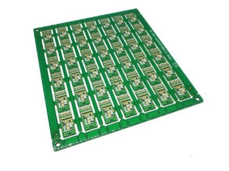
We manufacture high-precision 4-layer PCBs for a variety of applications, including consumer electronics, automotive, and telecommunications. Our commitment to stable quality and consistent performance ensures reliability for your repeat production needs.
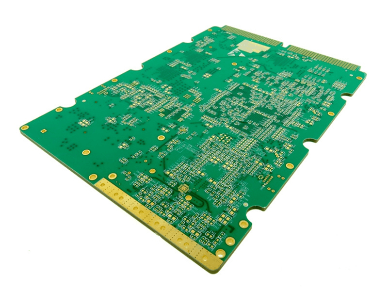
4-Layer PCB Capabilities
4-Layer PCB Process Capability
-
Layer Count
4 layers
-
PCB Dimensions
≤24*48inch(610*1220mm)
-
Materials Types
FR-4 | High Tg | Halogen-free | PTFE | Ceramic PCB | Metal substrate material
-
Material Brand
Lianmao | Shengyi | Taiyao | Nanya | Panasonic | Isola | Nelco | Rogers | Taconic | Arlon...
-
Board Thickness
0.2mm-8.0mm
-
Finish Treatment
Immersion Gold|Lead-free HASL|OSP|Immersion Tin|Immersion Silver|Thick Gold Plating|Silver Plating|Immersion Gold+OSP
-
Copper thickness
0.5 OZ - 6 OZ
-
SolderMask Color
Green| Blue| Black|Yellow| Red|Purple| White...
-
Finish Treatment
Immersion Gold|Lead-free HASL|OSP|Immersion Tin|Immersion Silver|Thick Gold Plating|Silver Plating|Immersion Gold+OSP
Why Choose Us for 4-Layer PCB Manufacturing
We support engineers with reliable 4-layer PCB manufacturing,
from prototype builds to stable repeat production.
Every 4-layer PCB undergoes a thorough review by our engineers to ensure proper stack-up, impedance control, and manufacturability before production begins.
We prioritize consistent quality across all batches, providing reliable support for both prototypes and long-term production needs.
Our extensive experience allows us to handle tight trace/space requirements, controlled impedance, and precise multilayer lamination for complex designs.
We offer clear technical communication and prompt responses, ensuring effective support for overseas engineering and purchasing teams.
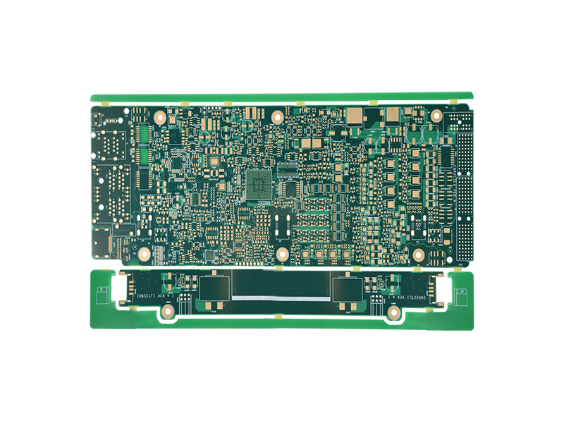
Related Project We Had Done
4-Layer PCB for Industrial Control System
Application
Industrial Control
Key Specs
Challenge
Result
4-Layer PCB for Industrial Power Control
Application
Key Specs
Challenge
Result
4-Layer PCB for IoT Gateway Device
Application
IoT Gateway & Communication Device
Key Specs
Challenge
Result
Quality Control & Certifications for 4-Layer PCB Production
Common Questions
Most Popular Questions
What is the typical lead time for 4-layer PCB production?
Prototype lead time is typically 7–10 working days.
Mass production lead time depends on quantity and specifications.
How thin can a 4-layer PCB be manufactured?
The minimum board thickness for our 4-layer PCBs is 0.2 mm, allowing for compact designs.
What surface finishes are available for 4-layer PCBs?
Options include immersion gold, lead-free HASL, OSP, and immersion silver, among others, to meet specific performance and reliability needs.
What types of testing do you perform on 4-layer PCBs?
We conduct extensive testing, including electrical testing (E-Test), automated optical inspection (AOI), and functional testing to ensure quality and reliability.
How quickly can I receive a quote for a 4-layer PCB?
We can provide a quote for your 4-layer PCB within 2 hours, ensuring a fast response to your project needs.
Send Us a Message
The more detailed you fill out, the faster we can move to the next step.

