
Circuit failures at high frequencies? Signal distortions ruining performance? Radio Frequency Printed Circuit Boards (RF PCBs) solve these modern engineering nightmares. These specialized boards handle frequencies between 100MHz and 300GHz, enabling critical technologies like 5G and satellite communications.
RF PCBs[^1] are printed circuit boards optimized for high-frequency signals (100MHz–300GHz) using low-loss materials like PTFE and Rogers laminates. They ensure stable impedance control and minimal signal distortion, outperforming standard PCBs in wireless communication, radar, and IoT systems.
Understanding RF PCBs requires analyzing their unique materials, design rules, and applications. Let’s break down the key elements that make these boards indispensable in today’s tech-driven world.
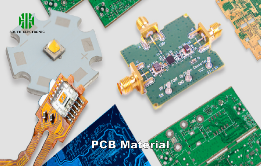
What Materials Are Essential for High-Frequency PCBs?
Ever wonder why your wireless router falters during video calls? Cheap PCB materials can’t handle high frequencies. RF PCBs demand substrates with minimal dielectric loss to maintain signal integrity[^2] under extreme conditions.
High-frequency PCBs require low-loss dielectric materials[^3] like PTFE, Rogers RO4000 series, or ceramic-filled laminates. These minimize signal attenuation while offering stable thermal properties. Copper foil with smooth surfaces reduces skin effect losses at high frequencies.
)
Choosing Materials for Signal Integrity
Material selection depends on three factors:
| Property | PTFE (Teflon) | Rogers RO4350B | Ceramic-filled FR4 |
|---|---|---|---|
| Dielectric Loss | 0.001 | 0.0037 | 0.02 |
| Cost | High | Medium | Low |
| Frequency Range | >30 GHz | ≤20 GHz | ≤6 GHz |
PTFE offers the lowest loss but struggles with mechanical stability. Rogers laminates balance cost and performance for sub-20GHz applications. For sub-6GHz IoT devices, ceramic-filled FR4 provides adequate performance at lower costs. Always prioritize dielectric constant consistency across temperature changes.
How Does Impedance Matching Impact RF PCB Performance?
Signal reflections causing data errors? Impedance mismatches disrupt RF systems. Even a 5% mismatch can reflect 10% of the signal, leading to power loss and noise.
Impedance matching[^4] ensures maximum power transfer between components. Mismatched traces cause signal reflections, distorting waveforms. Controlled impedance (±5% tolerance) is critical for maintaining signal integrity in RF circuits.
)
Balancing Impedance in RF Designs
Three factors influence impedance:
| Factor | Impact on Impedance | Solution |
|---|---|---|
| Trace Width | Narrower = Higher | Use 50Ω standard designs |
| Dielectric Thickness | Thicker = Higher | Adjust stackup pre-layout |
| Copper Weight | Thinner = Higher | Simulate with field solvers |
For example, a 1.6mm Rogers RO4350B board needs 0.25mm trace width for 50Ω microstrip lines. Use tapered transitions between different impedance sections. Always validate with time-domain reflectometry (TDR) testing.
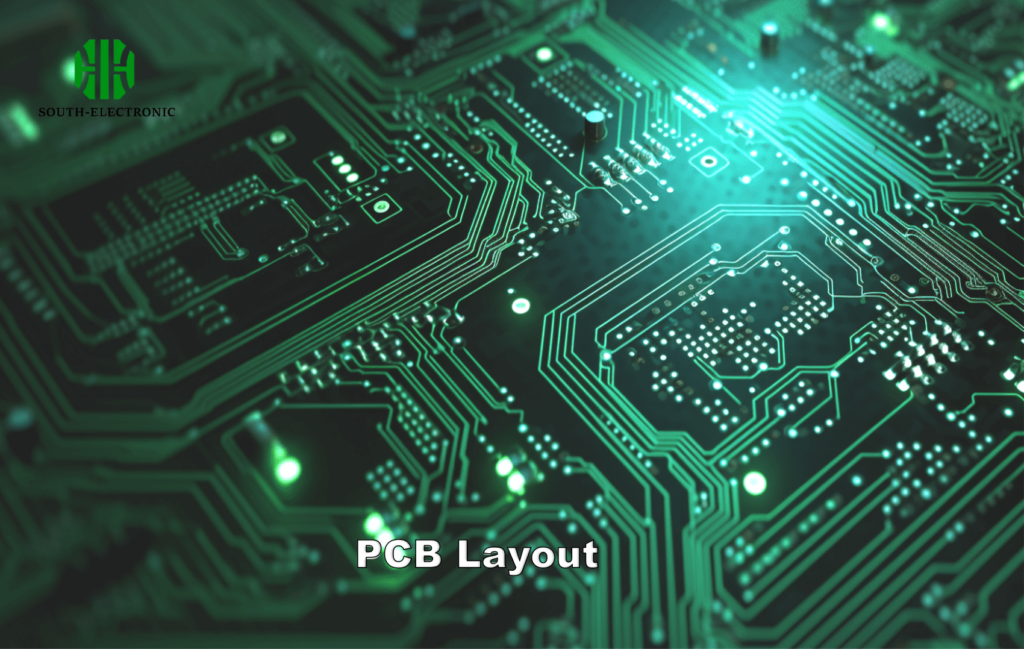
What Design Rules Prevent Signal Loss in RF Circuit Boards?
Crosstalk ruining your RF signals? Poor layout decisions amplify losses. RF PCB design demands precision in trace routing[^5], grounding, and shielding.
Minimize signal loss using short, straight traces with smooth bends (45° or arcs). Avoid vias in high-frequency paths—each via adds 0.5dB loss at 10GHz. Use continuous ground planes and guard rings to shield sensitive traces.
)
Zero-Loss Design Checklist
| Rule | Application | Benefit |
|---|---|---|
| Ground Via Fences | Around RF traces | Reduces crosstalk by 30% |
| Coaxial Feedlines | Antenna connections | Prevents impedance jumps |
| Differential Pairs | High-speed data | Cancels EMI noise |
Keep traces shorter than λ/10 at max frequency (e.g., 3mm for 10GHz). For multilayer boards, dedicate adjacent layers to ground. Simulate return current paths to avoid resonant loops.
Which Industries Demand High-Frequency PCBs?
Why do fighter jets avoid Wi-Fi drops? Mission-critical systems rely on RF PCBs. These boards enable technologies where failure isn’t an option.
Industries requiring high-frequency PCBs include telecommunications[^6] (5G base stations), aerospace (radar systems), medical (MRI machines), and automotive (ADAS sensors). Each demands reliability under extreme conditions.
Industry-Specific Requirements
| Industry | Frequency Range | Key Material | Use Case |
|---|---|---|---|
| Telecommunications | 3-30 GHz | Rogers RO4835 | 5G millimeter-wave |
| Aerospace | 8-40 GHz | PTFE with ceramic | Phased array radar |
| Medical | 1-10 GHz | IsoClad 933 (low outgassing) | MRI RF coils |
| Automotive | 24-77 GHz | Megtron 6 | Radar collision avoidance |
Aerospace PCBs prioritize thermal stability (-55°C to 200°C), while medical boards need biocompatible coatings. Automotive designs focus on vibration resistance.
Conclusion
RF PCBs power our connected world through meticulous material selection, impedance control, and loss-minimizing layouts. From 5G to radar systems, these boards enable technologies that demand precision at high frequencies. Stay ahead by mastering their design intricacies.
[^1]: Explore this link to understand how RF PCBs are revolutionizing high-frequency technology and their critical role in modern communications.
[^2]: Learn how material choices impact signal integrity, crucial for the performance of high-frequency PCBs.
[^3]: Discover the importance of low-loss dielectric materials in maintaining signal integrity for high-frequency applications.
[^4]: Understanding impedance matching is crucial for optimizing RF PCB performance and minimizing signal loss. Explore this resource for in-depth insights.
[^5]: Effective trace routing is essential to prevent signal loss in RF circuits. Discover best practices to enhance your PCB designs.
[^6]: Discover how telecommunications leverage high-frequency PCBs for advancements like 5G and beyond.

