
Ever damaged a circuit board through repeated use? Gold fingers solve this pain by creating ultra-durable connections that survive thousands of insertions in mission-critical systems.
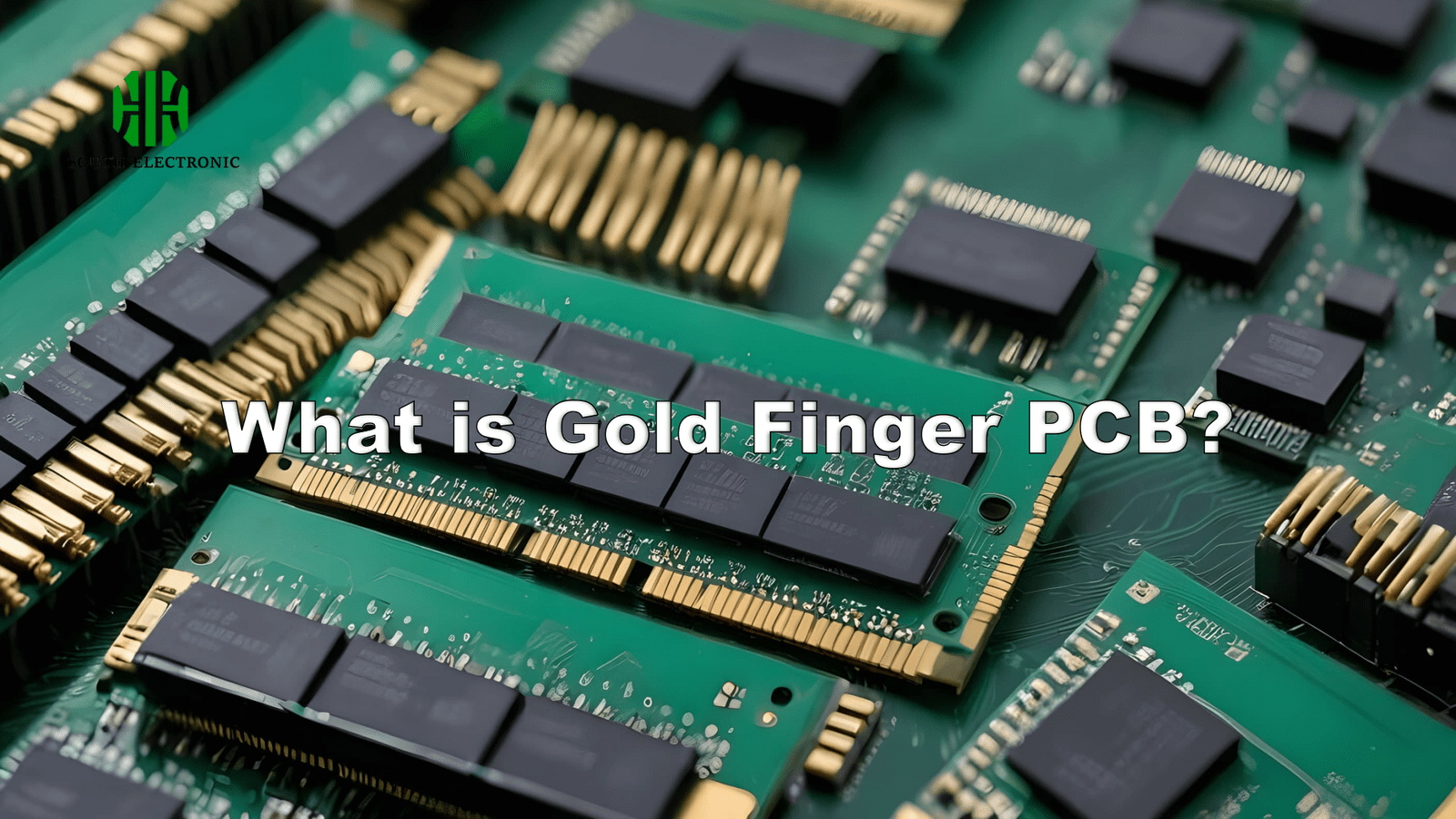
Gold finger PCBs use gold-plated edge connectors[^1] for reliable electrical contacts in demanding applications. These specialized contacts feature nickel undercoating, precise bevel angles, and meet strict IPC durability standards[^2] – making them essential for industrial/computing devices exposed to mechanical stress.
While gold fingers[^3] might look simple, their engineering reveals fascinating details. Let’s examine their key applications, technical specifications, and performance advantages over other contact materials.
How Are Gold Fingers Used?
Why do enterprise servers fail less than consumer electronics? The answer lies in gold fingers’ unique ability to maintain signal integrity through endless connection cycles.
Gold fingers primarily enable removable connections in high-use devices: PCIe cards, RAM modules, industrial test equipment. Their wear resistance prevents oxidation while supporting 30,000+ insertion cycles in vibration-prone environments.
)
Critical Application Requirements
| Use Case | Gold Thickness | Bevel Angle | Testing Standard |
|---|---|---|---|
| Consumer RAM | 2-5µ" | 30-45° | IPC-6013 Class 1 |
| Industrial Automation | 10-30µ" | 20-30° | IPC-6013 Class 3 |
| Military/Aerospace | 30-50µ" | 15-20° | MIL-PRF-55342 |
The plating thickness directly impacts durability. Industrial systems require 10-30 microinches of hard gold over 100-200µ" nickel underplating. Steeper bevel angles (15-20°) prevent edge snagging in high-vibration military applications, while consumer electronics use gentler angles to reduce production costs.
Gold Finger Specifications You Should Know
Not all gold plating is equal! Understanding these 3 specs separates professional PCB designs from amateur attempts.
Key specifications include 3-50µ" gold thickness[^4], nickel barrier layer[^5] (100-300µ"), and 15-45° bevel angles. IPC-6013 Class 2/3 standards require <100mΩ contact resistance[^6] and 25+ μm adhesion strength.
)
Technical Breakdown
Layer Composition:
- Base copper (0.5-2oz)
- Nickel barrier (100-300µ") – prevents copper migration
- Hard gold plating (3-50µ") – 99.7% purity cobalt-hardened
Performance Metrics:
- Contact resistance: <100mΩ after 10k cycles
- Microhardness: 130-200 HK25 (Knoop scale)
- Solderability window: 48hrs post-plating
Industrial clients often request selective plating – applying gold only on contact areas to reduce costs by 40-60% compared to full-edge plating.
Gold vs Other Contact Finishes
Silver and tin cost less, so why pay premium for gold? The hidden failures from "cheap" finishes will shock you.
Gold outperforms tin/silver in oxidation resistance[^7] and durability. Tin develops whiskers causing shorts (60% failure rate @ 5k cycles), while gold maintains <0.1% contact resistance change[^8] after 30k insertions.
)
Material Performance Matrix
| Finish | Cycles to 10% ΔR | Oxidation Rate | Cost Factor |
|---|---|---|---|
| Hard Au | 50,000+ | 0.02μg/cm²/yr | 10x |
| ENIG | 5,000 | 0.5μg/cm²/yr | 3x |
| HASL Sn | 1,200 | 2.3μg/cm²/yr | 1x |
| Ag | 8,000 | 1.1μg/cm²/yr | 6x |
Gold's initial 10x cost pays off long-term: Data centers using gold contacts report 92% lower maintenance costs[^9] over 5 years compared to tin finishes. The nickel underlayer prevents fretting corrosion – a key failure mode in DIN rail industrial controls.
Conclusion
Gold fingers offer unmatched reliability for critical connections, with proper specification being vital. Choose plating thickness and angles based on lifecycle requirements, and always verify against IPC/MIL standards.
[^1]: Learn how gold-plated edge connectors ensure reliable electrical connections, especially in demanding applications.
[^2]: Understanding IPC durability standards can help you ensure the quality and reliability of electronic components in your projects.
[^3]: Explore the significance of gold fingers in PCB design and how they enhance durability and performance in electronics.
[^4]: Understanding gold thickness is crucial for ensuring durability and performance in PCB designs. Explore this link to learn more.
[^5]: The nickel barrier layer plays a vital role in preventing copper migration, which is essential for PCB longevity. Discover more about its significance.
[^6]: Contact resistance is a key metric for PCB reliability. Learn how it impacts performance and what standards to meet for optimal results.
[^7]: Understanding oxidation resistance is crucial for selecting reliable materials in electronics, ensuring longevity and performance.
[^8]: Exploring contact resistance change helps in grasping its impact on device reliability and efficiency, essential for engineers.
[^9]: Investigating maintenance costs reveals the long-term savings and benefits of using gold finishes over cheaper alternatives.


