
Custom HDI PCB Manufacturing Services
Min trace 3/3 mil | ENIG / HASL | FR-4 & High-TG | AOI & E-Test
We manufacture high-precision HDI PCBs for automotive, medical, and consumer electronics, delivering stable quality and consistent performance for repeat production.
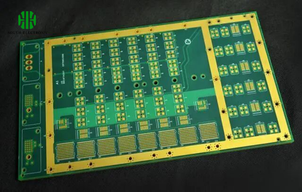
HDI PCB Capabilities
Rigid PCB Process Capability
-
Layer Count
1-68 layers
-
PCB Dimensions
≤24*48inch(610*1220mm)
-
Materials Types
FR-4 | High Tg | Halogen-free | PTFE | Ceramic PCB | Metal substrate material
-
Material Brand
Rogers | Isola | Nelco | Panasonic | Taconic | Arlon
-
Board Thickness
0.2mm-8.0mm
-
Finish Treatment
Immersion Gold | Lead-free HASL | OSP | Immersion Tin | Immersion Silver | Thick Gold Plating | Silver Plating
-
Copper thickness
0.33 OZ-8 OZ
-
SolderMask Color
Green | Blue | Black | Yellow | Red | Purple | White
-
Finish Treatment
Immersion Gold|Lead-free HASL|OSP|Immersion Tin|Immersion Silver|Thick Gold Plating|Silver Plating|Immersion Gold+OSP
Why Choose Us for HDI PCB Manufacturing
We support engineers with reliable HDI PCB manufacturing,
from prototype builds to stable repeat production.
Every HDI PCB is meticulously reviewed by our engineers to verify stack-up, micro via design, impedance control, and manufacturability before production.
We prioritize consistent quality across batches, ensuring reliable performance for both prototypes and long-term production runs.
Experienced in high-density interconnections, micro vias, and multilayer lamination for intricate and compact designs.
We ensure clear technical communication and prompt responses to effectively support overseas engineering and purchasing teams.
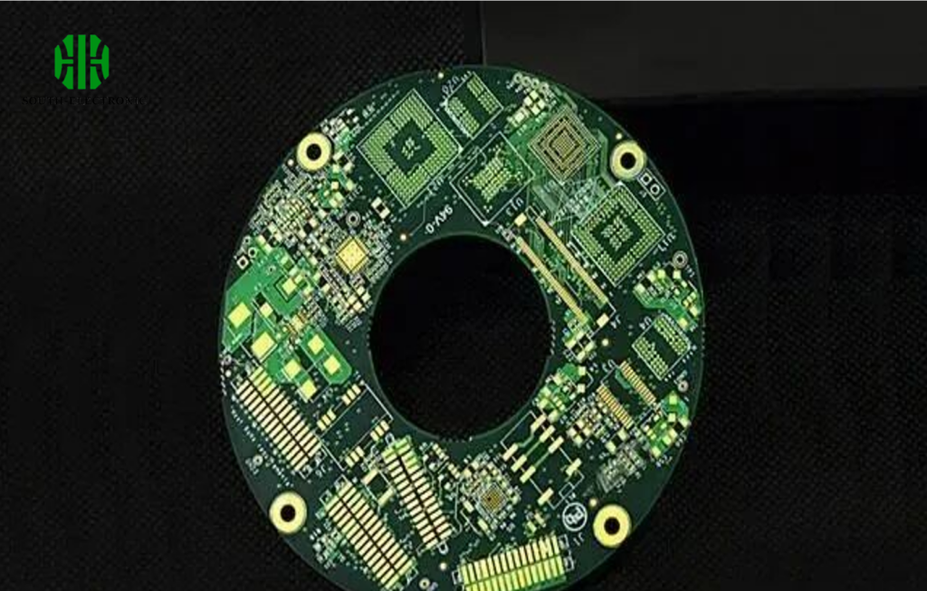
Related Projects We Have Done
HDI PCB for Automotive Control Module

Application
Automotive Control
Key Specs
HDI, micro vias, controlled impedance
Challenge
Space constraints and strict reliability requirements
Result
Consistent performance and durability in harsh environments
HDI PCB for Medical Device
Application
Medical Monitoring Equipment
Key Specs
HDI, high-frequency, impedance controlled
Challenge
High-density design with stringent regulatory compliance
Result
Reliable functionality and compliance for critical medical applications
HDI PCB for Consumer Electronics
Application
Smartphone and Tablet Devices
Key Specs
HDI, multi-layer structure, controlled impedance
Challenge
Compact layout and maintaining signal integrity for high-speed data transfer
Result
Enhanced performance and consistent quality for mass production
Quality Control & Certifications for HDI PCB Production
Common Questions
Most Popular Questions
What is the typical lead time for HDI PCB manufacturing?
Standard lead time is 2-3 weeks; express options available for urgent projects.
Do you offer prototypes for HDI PCBs?
Yes, we provide rapid prototyping services for HDI PCBs to test designs before mass production.
Can you handle complex HDI designs?
Absolutely! Our experienced engineering team specializes in complex HDI designs for manufacturability and reliability.
What kind of testing do you provide for HDI PCBs?
We offer extensive testing</strong> options, including electrical testing, functional testing, and automated optical inspection (AOI)
How can I get a quote for my HDI PCB project?
Request a quote easily through our website or by contacting our sales team; provide necessary specifications for a response within 2 hours
Send Us a Message
The more detailed you fill out, the faster we can move to the next step.
