

Many engineers struggle with frustrating antenna failures. Your wireless device might die before launch. This wastes time and money.
Ensure antenna clearance at the PCB edge, extend ground planes, use EM simulations, follow frequency guidelines, and validate with network analyzer tests. These steps prevent most common design errors.
Let me show you how these principles apply to key antenna challenges. You’ll gain practical solutions for your next project.
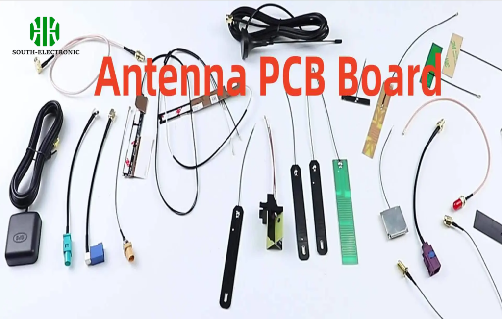
Which PCB Antenna Type is Best for Your Wireless Project?
Picking the wrong antenna cripples wireless performance. Your device could face range issues or signal drops. That kills user experience.
Match antenna type to your frequency, space limits, cost targets, and radiation pattern needs. Common choices include monopole, dipole, PIFA, or chip antennas for different scenarios.
Key Selection Factors
Every antenna type involves crucial tradeoffs. Ask these questions first:
| Factor | Why It Matters | Real-World Impact |
|---|---|---|
| Frequency | Antennas work only at specific bands | Wrong choice = 90% signal loss |
| Space | Larger antennas give better range | Tiny PCB? Chip antennas save space |
| Cost | Simple traces vs expensive ceramics | Mass production adds cost pressure |
| Radiation | Omnidirectional vs directional focus | Impacts device orientation limits |
For example, monopole antennas provide simplicity but need clearance space. PIFA designs work well in compact devices but require careful grounding. Always simulate radiation patterns before finalizing. If your design uses Bluetooth Low Energy, a small ceramic chip antenna might suffice for basic needs. But industrial IoT sensors needing long range demand inverted-F antennas which consume more board space. Remember to prioritize your top three performance requirements early. Test prototypes in actual metal enclosures – plastic cases change everything.
Can Simulation Tools Accurately Predict Real-World PCB Antenna Performance?
Simulations occasionally miss critical flaws. Your virtual model might show perfect results, but real devices fail. This causes expensive redesigns.
EM simulations provide reliable predictions when combined with material models, measured S-parameters, and real-world validation. They cannot replace prototyping in complex conditions.
Simulation Accuracy Factors
Tools need careful setup to reduce prediction gaps:
| Parameter | Simulation Limits | Mitigation Strategy |
|---|---|---|
| Material Models | Generic data ≠ actual PCB layers | Measure your board’s Dk and Df |
| Component Effects | Nearby traces alter performance | Include all critical components |
| Radiation Boundary | Enclosure changes antenna behavior | Model entire housing assembly |
| Manufacturing Variances | Tolerances shift resonance | Run tolerance analysis ±10% |
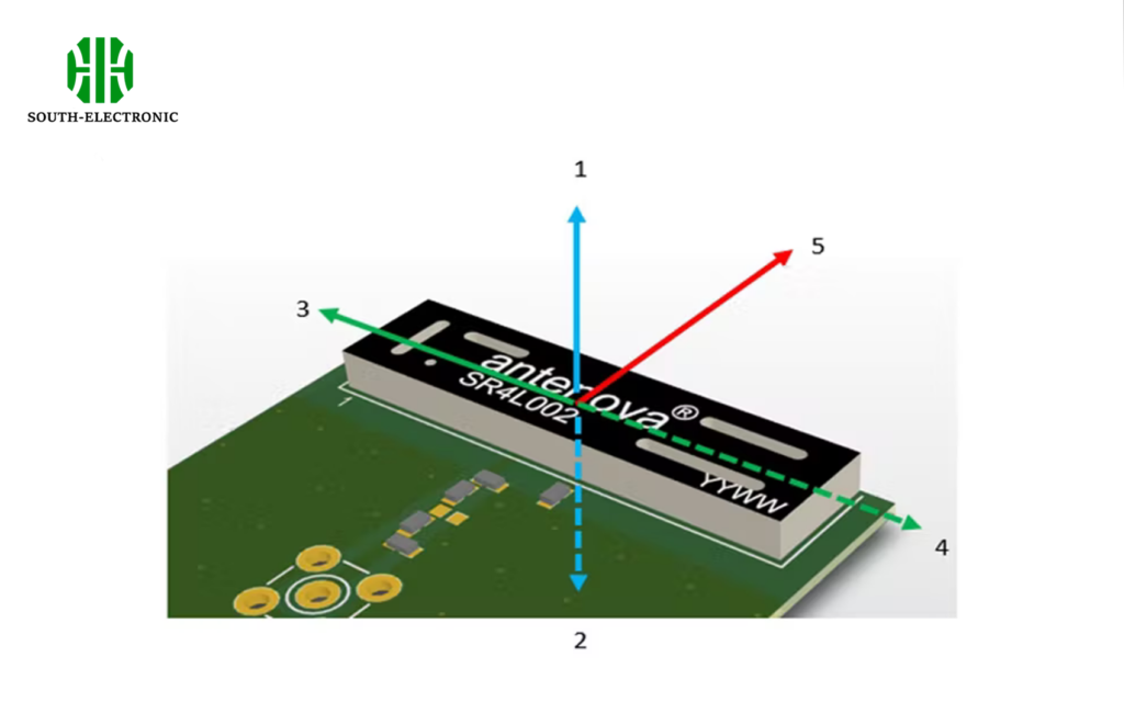
Always include your actual plastic casing in simulations. I once saw a perfect 2.4GHz simulation fail because the model omitted the metal battery case. Verify near-field radiation patterns with probe tests. Cross-check simulated S11 curves with network analyzer results. Remember antennas behave differently during transmission versus reception. If tools predict < -10dB return loss but measurements show -6dB, debug copper thickness or soldermask effects. Combine Momentum HFSS for board-level details and EMPro for 3D radiation patterns. Never skip physical verification.
How to Balance Cost and Performance in Custom PCB Antenna Design?
High-performance antennas often break budgets. You might overspend on unnecessary features. This inflates project costs unacceptably.
Start with minimum viable specs, prioritize key metrics like gain/swr, and prototype early. Avoid gold-plating solutions that exceed requirements.
Strategic Tradeoff Framework
Systematically evaluate where to cut costs:
| Cost Driver | High-Performance Choice | Budget Compromise | Risk Assessment |
|---|---|---|---|
| Materials | Rogers laminar ($) | Standard FR4 (¢) | Higher loss in humid areas |
| Complexity | Multi-layer design | Single side trace | Tuning needed post-production |
| Tuning | Laser trimming every unit | Fixed geometry with margin | Minor performance variance |
| Validation | Anechoic chamber testing | Field distance tests | Approximate pattern data |
Set clear performance thresholds first. For a consumer thermometer needing 3-meter range, optimize for manufacturability over peak efficiency. I saved 40% on a medical device project by switching from ceramic to trace antennas after proving -12dB return loss sufficed. Always prototype the antenna isolated from other circuits first – EMI interference often masks cost-saving opportunities. Use free EM tools like QUCS for initial tuning when budget constraints hit hard. Document every compromise so teams understand limitations later.
Conclusion
Avoid PCB antenna errors by combining smart placement, rigorous simulations, cost-focused choices, and real testing. These fundamentals deliver reliable wireless performance.

