PCBs are the foundation of electronic devices, and it’s important to know how different elements like nets and via holes work together for good PCB design. In this article, we’ll look at the relationship between nets and via holes, what they do in PCB design, and how to manage them.
What is a Net on a PCB?
In PCB design, a net is a collection of electrically connected points, such as pads or pins, that are meant to carry a particular electrical signal. Nets are important because they define how components on a PCB are connected.
Nets are like the “wiring” inside a PCB that makes sure all the necessary components are connected correctly. For example, a Ground (GND) net might connect all the ground pins on different components to make sure there’s a common return path for current.
Nets are defined during the schematic phase of PCB design. During this phase, the designer says which pads or pins need to be electrically connected. Then, those connections are translated into the PCB layout, where they’re physically routed on the board.
Example of Common Nets
| Net Name | Description |
|---|---|
| GND | Connects all ground pins to a common ground. |
| VCC | Distributes power supply to various components. |
| SIGNAL_1 | Carries a specific signal between components. |

What is the Difference Between a Via and a Hole in PCB?
When you’re talking about PCB design, you need to know the difference between vias and holes. They do different things in the board.
Plated Through-Holes (PTHs)
Plated through-holes (PTHs) are holes that go all the way through the PCB and are plated with copper. They are usually used to mount through-hole components like resistors, capacitors, or ICs.
Vias
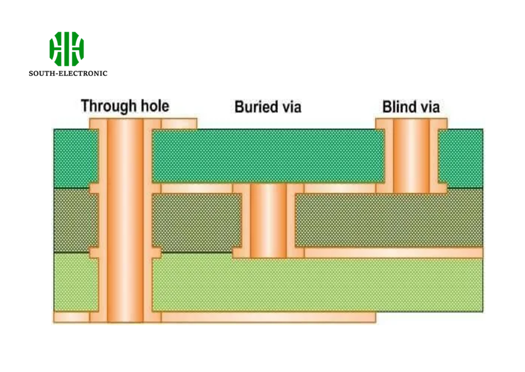
Vias, on the other hand, are much smaller holes used exclusively for routing signals or power between different layers of a multilayer PCB. Unlike PTHs, vias are not intended for mounting components. There are several types of vias, including:
- Through Vias: Pass through all layers of the PCB.
- Blind Vias: Connect an outer layer to one or more inner layers but do not pass through the entire board.
- Buried Vias: Connect only inner layers and are not visible from the outer layers.
Key Differences Between Vias and PTHs
| Feature | Via | Plated Through-Hole (PTH) |
|---|---|---|
| Purpose | Routing signals/power | Mounting components |
| Location | Any layer(s) | Entire PCB thickness |
| Visibility | Not always visible | Visible on both sides of the PCB |
| Example Use | Layer-to-layer connection | Soldering a resistor or capacitor |

Best Practices for Managing Nets and Vias in PCB Design Tools
Knowing how to use PCB design tools effectively is critical when it comes to managing nets and vias. Tools like Altium, KiCad, or Eagle have features that make these tasks easier.
Nets Management
- Net Classes: Use net classes to group similar nets (e.g., all power nets) and apply consistent design rules.
- Clearances: Set appropriate clearances between different nets to avoid short circuits and crosstalk.
Vias Management
- Via Types: Choose the appropriate via type based on your design requirements.
- Via Placement: Use automated tools to place vias accurately and consistently.
Tips for Effective PCB Design
- Review DRC (Design Rule Check): Always run a DRC to catch errors in net connections and via placements.
- Use Via Stitching Wisely: Implement via stitching in areas where signal integrity or thermal management is critical.
- Documentation: Keep thorough documentation of net names and via placements for future reference and debugging.
Nets are what connect components, while vias are what allow those connections to extend across multiple layers of the PCB. By following best practices in managing these elements, you can ensure your PCB design is both functional and reliable.


